![[MAFT 2026 | H2 Technology Seminar] "Crystal" Moving into the Future: The Next Wave of Technological Revolution from Memory, Silicon Photonics to Quantum Computing](https://www.matek.com/upload/news_support_list_pic2/enL_news_support_26G31_BkwYGqWL60.png)
[MAFT 2026 | H2 Technology Seminar] "Crystal" Moving into the Future: The Next Wave of Technological Revolution from Memory, Silicon Photonics to Quantum Computing
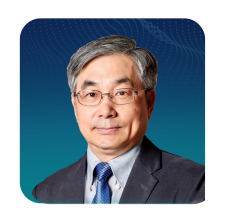
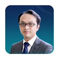
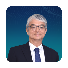
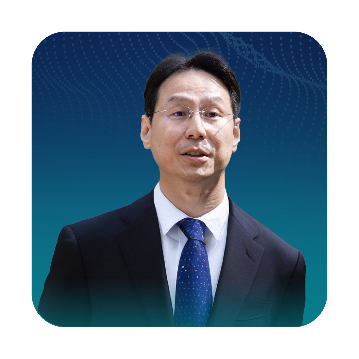
This MAFT seminar focuses on the core theme of "Innovative Components & Packaging," inviting experts from Tsinghua University, National Yang Ming Chiao Tung University, and National Cheng Kung University to focus on forward-looking topics such as superlattice ferroelectric memory, silicon photonics, 6G high-frequency EMI packaging, and quantum computing, guiding attendees to gain an in-depth understanding of the development trends of next-generation semiconductor technology.
We sincerely invite you to join us in exploring the key breakthroughs in future chip technology with industry and academic experts, and to seize the core opportunities of the next wave of semiconductor innovation!
Registration website:https://forms.office.com/r/9P8UAXEU9c
Kind reminder: Due to limited seating on-site, if the number of registrants is full, we will notify you to participate online. We appreciate your understanding and support.
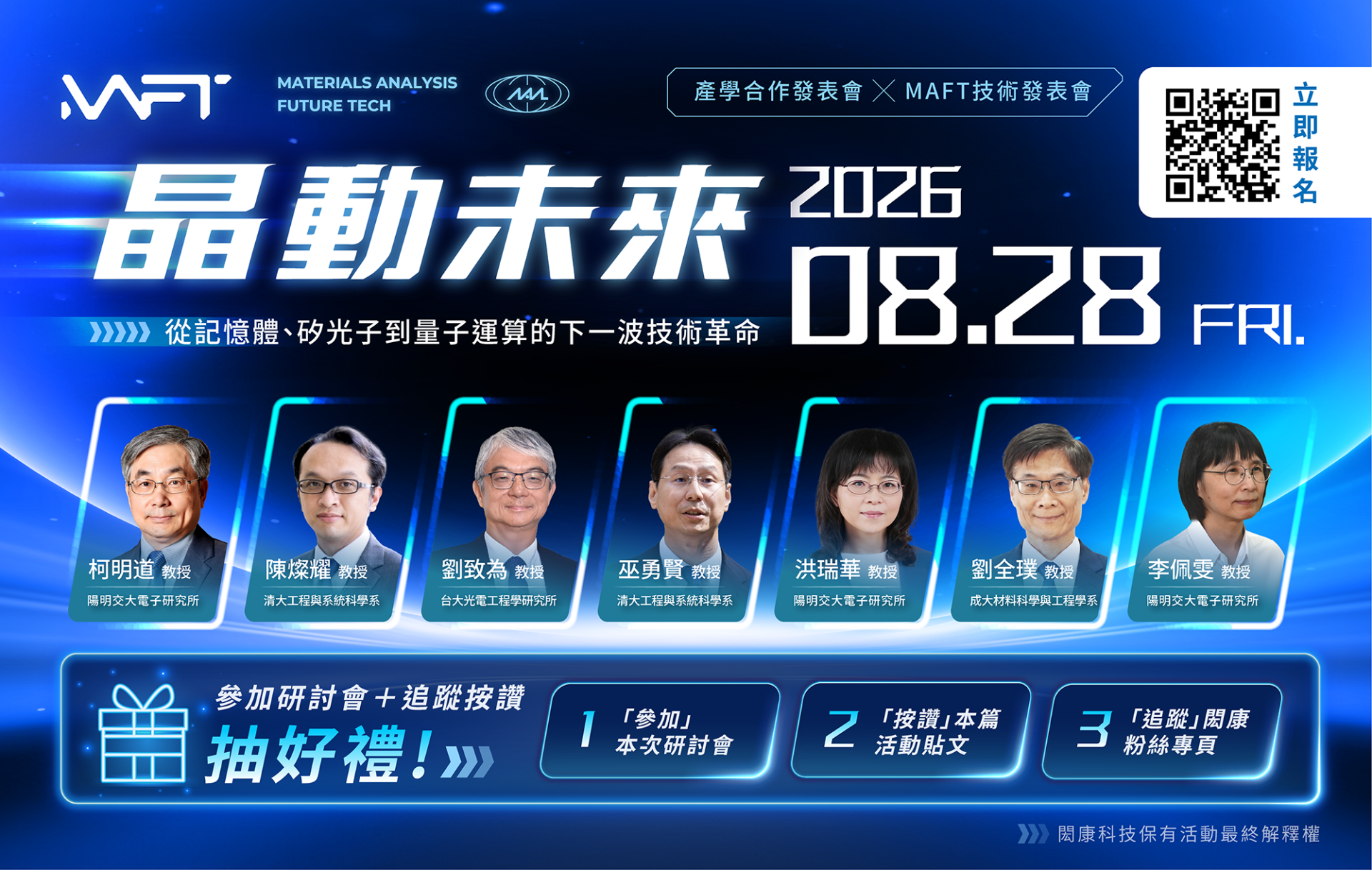
Complete 3 steps to draw great prizes!
1. Complete event registration and sign in on the day.
2. Like Facebook event-related posts
3. Follow MA-tek Facebook fan page (https://www.facebook.com/matek.analysis/)
|
Time |
Speaker |
Theme & Outline |
|
|---|---|---|---|
| Morning - Industry-Academia Collaboration (Physical Event) | |||
| 09:30~10:00 | Check-in | ||
| 10:00~10:20 | Opening & Guest Speech & Group Photo | ||
| 10:20~10:40 |
National Yang Ming Chiao Tung University Professor Ko Ming-Tao |
Innovative design of bipolar electrostatic discharge protection applied to the gate of GaN power devices | |
| 10:40~11:00 |
Tsinghua University Professor Chen Can-yao |
Atomic-level oxygen defects drive oxide metal nano-heterojunction catalysts for high-efficiency alkaline fuel cells. | |
| 11:00~11:20 |
National Taiwan University Professor Liu Zhiwei |
Gate-All-Around Nanosheet Stacking with GeSi and Oxide Semiconductor Channels using HZO Gate Stack for Advanced Logic and Memory Integration | |
| 11:20~12:00 |
Poster Exhibition and Discussion |
||
| 12:00~13:00 |
Lunch gathering |
||
|
Afternoon - MAFT Seminar(In-person/Online Event) |
|||
| 13:00~13:20 |
Check-in |
||
| 13:20~13:30 |
Opening |
||
| 13:30~14:30 |
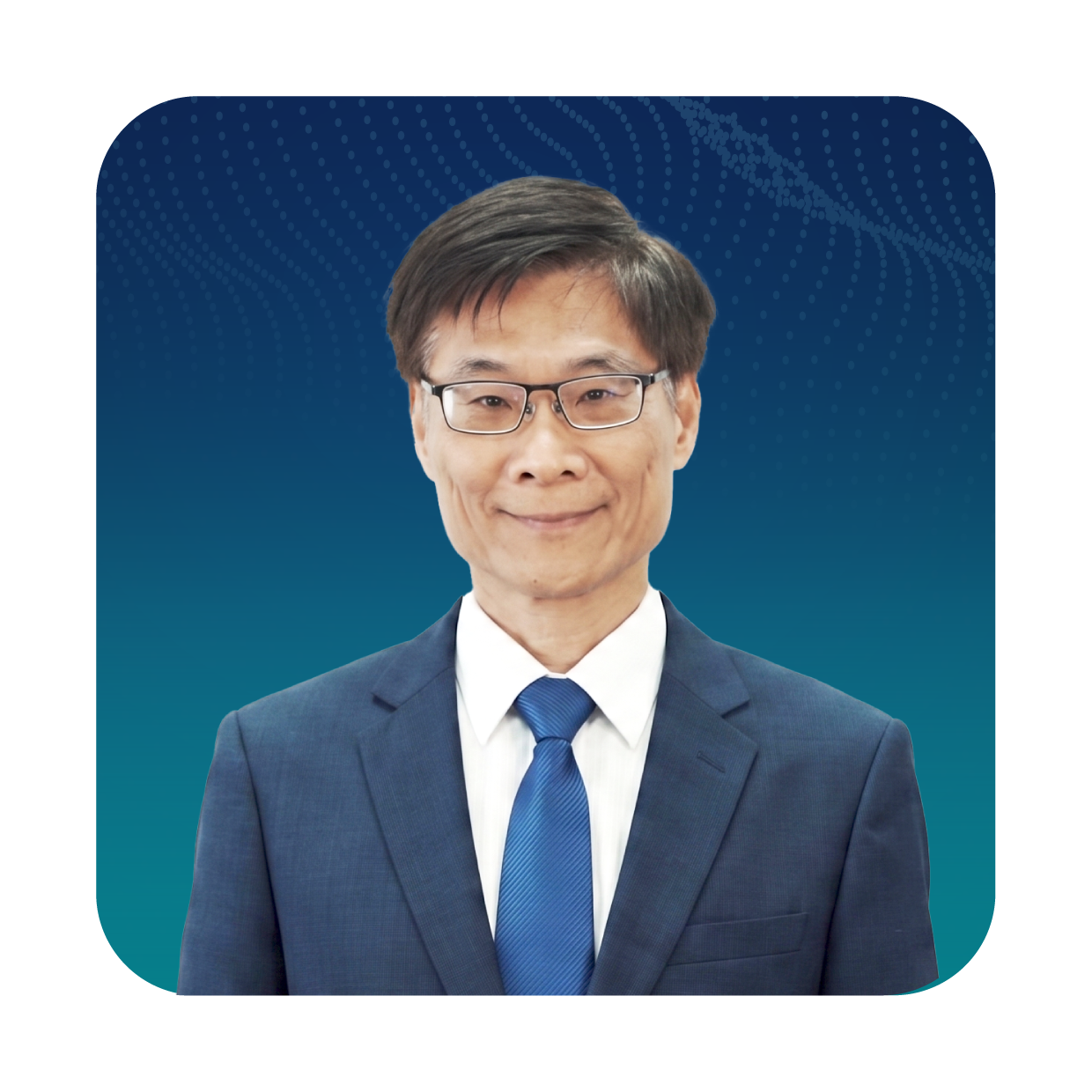
Tsinghua University Professor Wu Yong-Hsien
|
Topic: From Radiation Resistance Challenges to Reliability Design: Development Opportunities for Ferroelectric Memory in Future Space Electronics |
|
|
With the rapid development of low Earth orbit satellites, Space Edge Computing, and Agentic AI, the demand for high-performance, low-power, and radiation-hardened non-volatile memory in future space systems is increasing. Compared to traditional flash memory that stores data using charge, ferroelectric field-effect transistor memory (FeFET) uses the direction of ferroelectric polarization as the information carrier, offering advantages such as low voltage operation, non-destructive reading, and excellent radiation resistance potential. Therefore, it is regarded as an important candidate technology for the next generation of space electronics and intelligent computing systems.
This presentation will first introduce the main damage mechanisms of radiation on semiconductor devices, including total ionizing dose (TID), single event effects (SEE), and reliability issues caused by oxygen vacancies and interface defects. It will then explain the development history of radiation-resistant ferroelectric memory based on HfO₂ and share the systematic results of our research team's recent studies on HfZrOₓ (HZO) FeFET radiation resistance, including interface engineering (AlON interface layer), channel engineering (p-type and Ge channels), ferroelectric material composition engineering (Zr concentration optimization and composition gradient HZO), and high-energy proton radiation verification. At the same time, this presentation will also introduce the innovative superlattice + solid solution stacked structure developed in collaboration with MA-tek, and further explore its application potential in radiation-resistant ferroelectric memory, highlighting the critical role of advanced material analysis, process structure design, and defect engineering in next-generation reliability engineering, as well as the importance of establishing a radiation-resistant memory design framework.
Finally, from the perspective of future applications, we will explore the development potential of ferroelectric memory in application scenarios such as autonomous satellite systems, space edge computing, and future Space Data Centers. |
|||
| 14:30~15:30 |
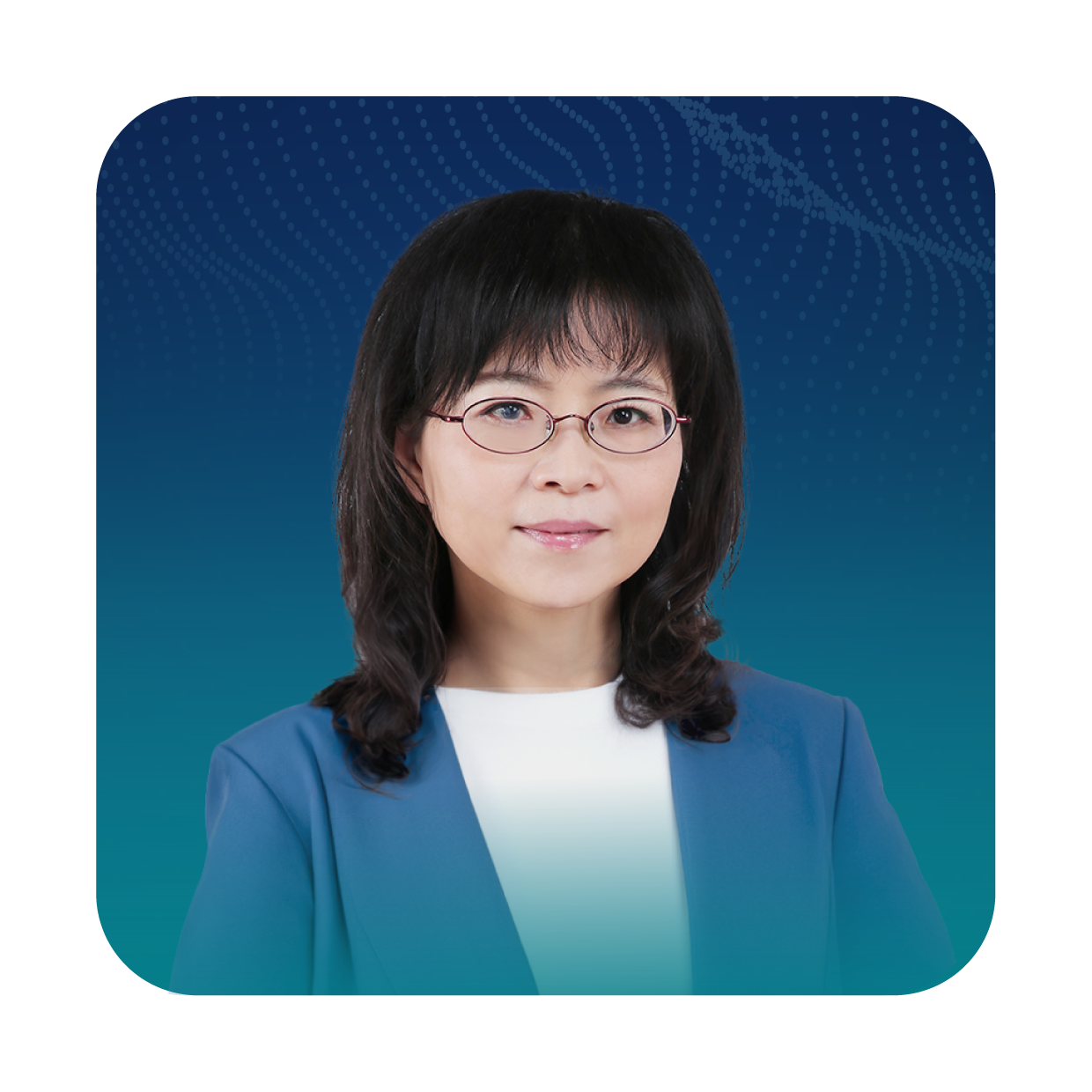
National Yang Ming Chiao Tung University Professor Hong Ruihua
|
Topic: High-speed transmission and silicon photonics heterogeneous integration technology | |
|
This topic covers a comprehensive analysis from technological drivers, core packaging evolution, heterogeneous integration methods to the industrial ecosystem.
1. Technological Driving Force: The Transmission Revolution Brought by AI/ML
2. The evolution of packaging architecture: from plug-in to Co-Packaged Optics (CPO)
3. Core Integration Technology: Silicon Photonics and Heterogeneous Integration
4. Emerging Interconnect Technology Applications
5. Industry Ecosystem and Prototyping Platform
6. Patent Distribution and Technology Validation
|
|||
| 15:30~16:00 |
Networking & Break |
||
| 16:00~17:00 |
National Cheng Kung University Professor Liu Quanpu
|
Topic:Advanced Packaging and Electromagnetic Protection Materials in the 6G Era |
|
|
With the rapid evolution of autonomous vehicle technology, vehicles are no longer just a means of transportation, but have become highly intelligent mobile platforms. From sensors to control units, from communication modules to artificial intelligence (AI) chips, every automotive module plays an indispensable role. In this technological revolution, "module verification" has become a key link to ensure safety, stability, and reliability.
At present, automotive module verification is divided into two main categories within the AEC-Q verification family: Multichip Module (MCM) and Optoelectronic Multichip Module (OE-MCM), referring to standards such as AEC-Q104 and AEC-Q102-003. The verification framework is divided into general commonality verification and special verification. Due to the wide variety of automotive module types, there are often issues with the applicability of certain test items. Therefore, it is essential to have a professional verification experience like that of MA-tek to tailor verification solutions that meet the standards, allowing automotive modules to quickly and confidently enter the new era of intelligent driving! |
|||
| 17:00~18:00 |
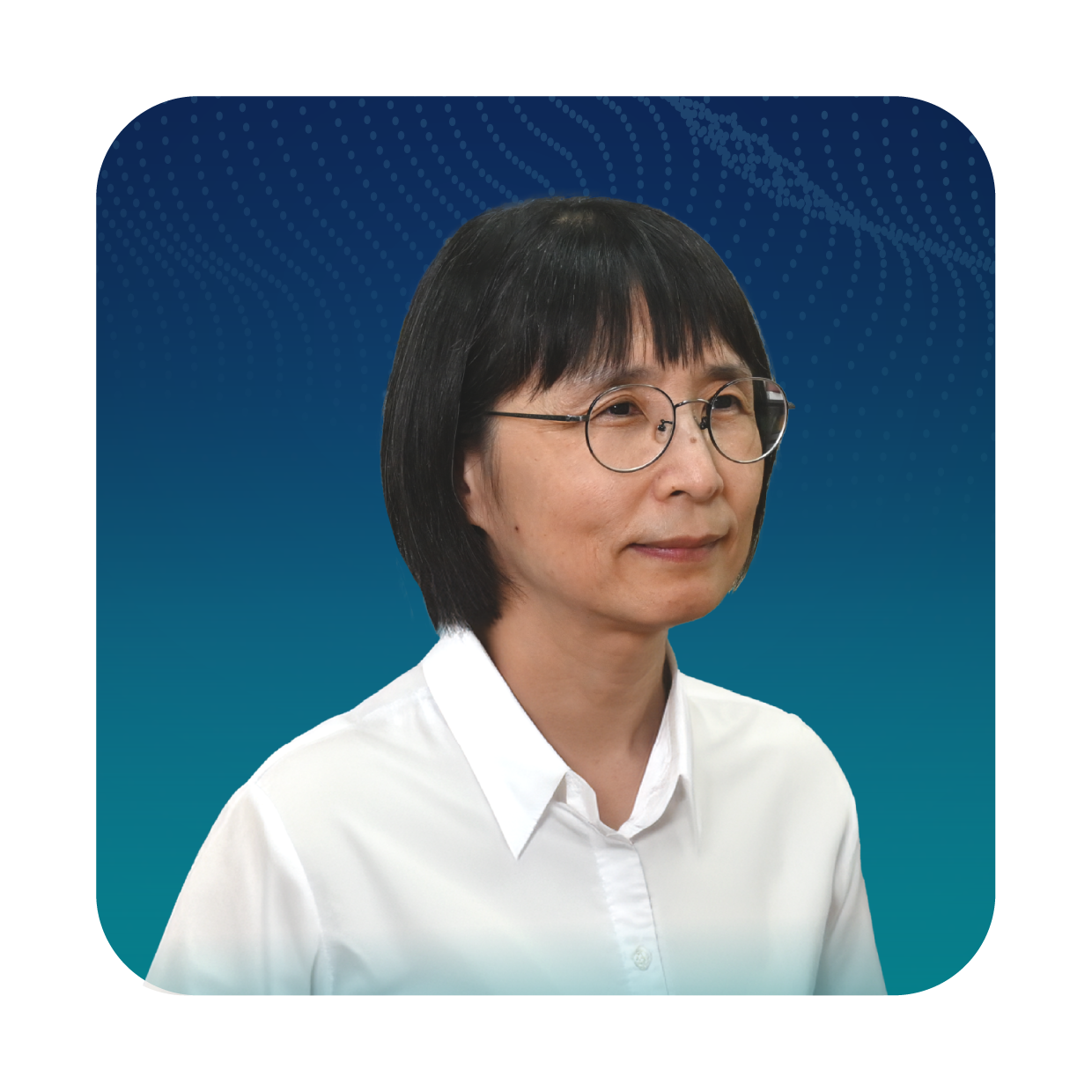
National Yang Ming Chiao Tung University Professor Li Pei-wen
|
Topic:Material Defined Germanium Quantum-dots for High Performance Quantum Computing |
|
|
The holy grail for implementing semiconductor quantum computing hardware is to take full advantage of robust CMOS manufacturing technology and operate at benign environment. Motivation to use Si/Ge quantum-dots (QDs) for implementing CMOS-integrable qubits and their charge/photon sensors is strong in light of the advanced CMOS and Si photonics technology, which allows full integration of qubits with CMOS control/readout circuitry and is beneficial to facilitate progress toward large-scale quantum computers. Remarkable achievements have been realized on Si/Ge spin qubits by forming fine metal-gates over Si/Ge or Si-MOS quantum-well structures. However, Si/Ge gate-defined spin qubit operation is limited at milli-Kelvin temperatures due to the challenge in forming sufficiently high potential barriers separating the Si/Ge QDs. On the other hand, material-defined QDs promise higher temperature operation and better immunity to quantum leakage. However, the holistic device and technology co-design of QDs, barriers, and control gates all in nm-scale is a formidable task. Another technical challenge lies in detecting minuscule signal of quantum states due to strong charge confinement wherein. |
|||
| 17:50~18:00 |
Event lottery & Return |
||