
Integrated Circuit Electrostatic Protection and Latch-up Testing Plan and Failure Verification Process
Every product has its lifespan, or we can say whether the reliability of this product is good or not. If it can be used for several years without damage until the next generation of products comes out, then we can say this product has good reliability. Conversely, if the usage time does not reach the level that this product should have, the reliability is poor. So how do we measure the reliability of a product? Basically, we will consider the conditions of the usage environment, such as voltage, temperature, humidity, or any adverse factors in the environment, and substitute them into the failure model to estimate the lifespan.
In the environment we are in, static electricity is an omnipresent killer. Since static electricity cannot be completely prevented, in order to safely withdraw when charges flow through the integrated circuit, the IC design will incorporate electrostatic discharge (ESD) protection circuits next to the pins to protect the chip, just like setting up a lightning rod at the top of a building. When lightning strikes the building, it can divert the charge and ensure that the electrical appliances inside the building are not damaged. Additionally, due to the structural characteristics of components, the so-called latch-up (LU) effect can cause large currents in the integrated circuit during operation, leading to functional problems and even permanent damage to the chip. Similarly, it is necessary to avoid LU issues in chip design.
In order to verify the protective capabilities of ESD and LU, the first task is to utilize specialized testing equipment, following the conditions and procedures defined by international standards, to confirm the reliability of integrated circuits under ESD and LU. If the circuit component fails to pass the ESD and LU tests, and the reasons for the failure have been identified, how to reinforce the chip design becomes the second task. This article elaborates on the preparation matters, judgment criteria, and the root cause analysis process after component failure regarding ESD and LU for these two tasks.
Data preparation before testing
Before conducting ESD and LU tests for the first time, common issues encountered include how to plan the testing scheme and execute it, as well as how to communicate the testing scheme with the project supervisor. To enhance communication efficiency between both parties, information can be provided based on the following topics.
Testing specifications
Before conducting tests, it is necessary to set the international standards to be followed. The formulation of these standards has its theoretical basis, thus ESD/LU test verification represents the acquisition of customer trust and assurance of usability. Below are the different testing projects and their corresponding international standards.
- HBM:
MIL-STD: Component types and some driver ICs
AEC-Q100 or AEC-Q101: Automotive Certification
JEDEC: The rest all use consumer product specifications
2. CDM:
ANSI/ESD SP5.3.2: This is the SCDM testing specification, currently only a few customers of driver ICs will test SCDM upon request.
AEC-Q100 or AEC-Q101: Automotive Certification
JEDEC: The old specification JESD22-C101F and the new specification JS-002-2022, the vast majority of products use the consumer product JEDEC, and it is recommended that customers follow the latest JS-002-2022.
3. LU:
JESD78F : Consumer Products
AEC-Q100 : Automotive qualification certification
Test conditions
- HBM: It is recommended to start from 500V and proceed to 1KV, 2KV, 4KV, and 8KV.
- CDM: The JEDEC safety standard is 500V, while AEC-Q100 additionally increases the standard for Corner Pins to 750V (Figure 1). The recommended voltage testing ranges are 250V, 500V, 750V, and 1000V in order.
- LU: Basically, according to the specifications, it is only necessary to achieve signal pin +100mA / -100mA, and for the power pin, it should be set to 1.5*VDDmax. The industry habit is to test one level higher, up to 200mA. In addition, it is necessary to provide the rated voltage and limit values for the setting of operating conditions.
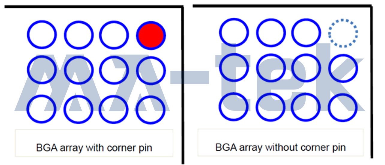
Figure 1 is a schematic diagram of the Corner Pin of the BGA package. The left image shows a design with Corner Pin, located at the red circle, which requires a CDM test standard of 750V. The right image shows a design without Corner Pin.
Number of tests
HBM /CDM / LU: According to the specifications, it is recommended that each test condition data should have 3 samples.
IC Package Outline Drawing (POD)
It is necessary to provide the names of the test pins, the pin types (Input / Output / IO / Power / GND), and their arrangement positions to facilitate the assessment and analysis of time and condition settings, which also serve as the basis for making test fixtures.
HBM test combination
When selecting MIL-STD specifications, all four test combinations in the first row of Table 1 can be chosen. Under this specification, the Power/Ground of each Power Domain can be connected together. When selecting JEDEC specifications, there are options for Table 2A or 2B. The Power/Ground of the same Power Domain can be connected to each other, but the Power/Ground of different Power Domains cannot be connected. Based on this, all IO pins apply ESD to different Power Domains, which corresponds to Table 2B, while IO pins only apply ESD to their own Power/Ground corresponds to Table 2A. If the most rigorous test conditions are to be used, or if it is unclear which test combination to use or for automotive regulation verification, it is recommended to use Table 2B. As for the automotive regulation AEC-Q100 certification, if the number of package pins is less than or equal to 6, then any combination of 2 pins must be verified.
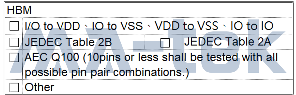
Table 1: The first row is the test combinations between IO and Power/Ground, and the second and third rows are the specifications to be adopted.
Special testing requirements for LU
The purpose of the LU test is to observe whether abnormal signal interference leads to the phenomenon of large current excitation. Therefore, after considering the actual conditions that may occur under the set test conditions and environment, some customers will select certain conditions for LU testing, as described below.
High Temperature Testing
At high temperatures, due to increased leakage current, it is easy to trigger the parasitic Silicon Controlled Rectifier (SCR) to start and produce the LU effect. Therefore, two test environments can be selected: room temperature or high temperature (depending on the maximum operating temperature of the product specifications or Tj temperature). The AEC specification mandates high-temperature testing.
Quiescent Current
High Performance Computing (HPC) ICs have higher Quiescent Current. As the market share of such ICs gradually increases, LU testing machines can no longer meet the high current requirements, and it is necessary to custom-make High Current LU fixtures and external high-power measuring instruments.
Pattern
General IC LU testing is a static test, where the input voltage and current are fixed values. However, the actual operation of the IC is dynamic, with periodic changes in high and low voltage at the input and output pins. Therefore, the input pattern under LU testing is designed to simulate the real operational behavior of LU under dynamic input conditions in the IC.
Test Pass/Fail Criteria
HBM and CDM testing according to the specifications requires testing the complete test items, including Parametric Testing and Functional Testing, in order to capture failure phenomena caused by ESD damage. In terms of Parametric Testing, on the Automatic Test Equipment (ATE), it tests Open/Short (OS), leakage current, and static current at the Power terminal. However, if using an ESD testing machine to compare the differences before and after ESD testing in real-time, two methods can be used for measurement. The first method measures the voltage when the current is equal to 1uA; if the difference before and after is less than 30%, it is considered passed through ESD testing, as shown in Figure 2. The second method is the Curve Compare Envelope, using the IV curve before ESD testing as a reference, and adjusting the maximum voltage and current by ±10% as the adjustment value. By adding this ± value to the IV Curve before testing, a range can be obtained; as long as the post-test IV falls within this range, it is considered passed through ESD verification, as shown in Figure 3.
-
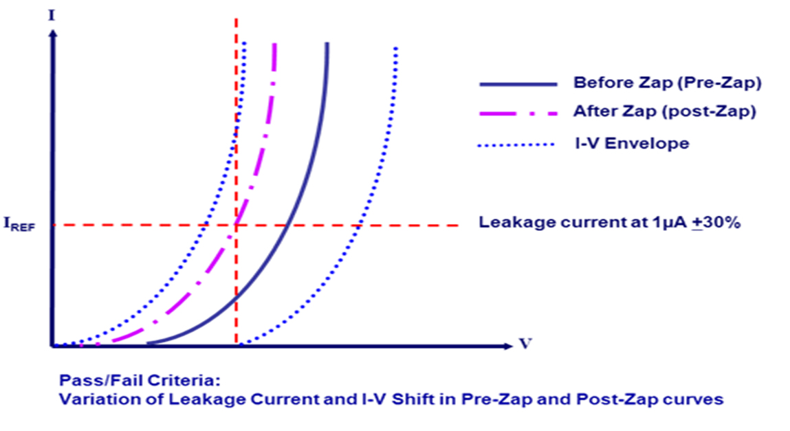 Figure 2 shows the IV changes before and after Zap. If the voltage change at 1uA reaches 30% or more, this pin is determined to be ESD Fail.
 -
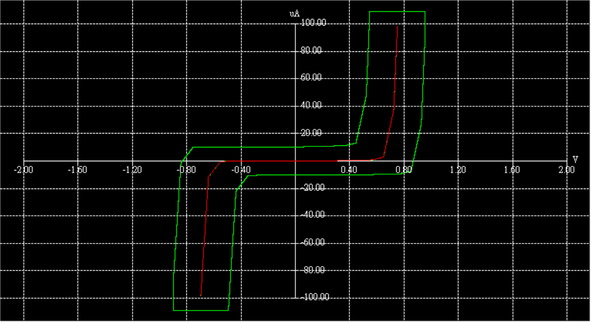 Figure 3 is a schematic diagram of the envelope. If the IV curve after Zap exceeds the range outlined by the green line, this pin is determined to have ESD Fail.
The Pass judgment criteria for LU is that if the current before measurement is INOM, then the maximum value between 1.4xINOM and INOM+10mA should be taken; if it is less than this value, it is considered validated.
Analysis and Solutions for ESD Verification Failures
According to the failure principles and experiences of ESD, when the overcurrent or overvoltage generated by electrostatic discharge exceeds the component's tolerance, it will result in the phenomenon of component burning. The form of component burning is determined by the discharge path, such as junction leakage, gate oxide breakdown, breakdown between drain and source, or breakdown between two different components, etc. In severe cases, the burning may extend upwards towards the metal layer. Since it is a case of component burning, it is basically suitable to use Photon Emission Microscopy (PEM, commonly known as EMMI) to locate the burning position. Additionally, OBIRCH, due to its ability to detect changes in resistance, can also be considered as a positioning tool if further confirmation of the burning position is needed.
The location of the electrostatic discharge burn can generally be divided into two categories based on the circuit where it occurs: ESD circuit (IO Cell) and internal circuit. As shown in Figure 4, the burn of the IO Cell can be understood as the ESD circuit performing the role of current diversion, preventing electrostatic discharge from damaging the internal circuit. However, if the overcurrent exceeds the tolerance of the ESD circuit, burning occurs. This type of burn corresponds to abnormal Pin legs in parameter testing, making it relatively easier to locate the burn position.
According to the theory of full crystal surface protection, when electrostatic discharge does not follow the expected conductive IO Cell but instead travels along other faster and more vulnerable paths, it may damage the internal circuits. At this point, it is necessary to use localization tools to identify the burned components in order to understand the discharge path for further design blocking.
To summarize the above description, to confirm burnt components or circuits, there are several options as follows.
- If the damaged circuit is known to be in the IO Cell, for quick confirmation, a Total Delayer can be executed, and then observed using an Optical Microscope (OM) or Scanning Electron Microscope (SEM), as shown in Figure 5.
- Using hotspot localization tools, EMMI or OBIRCH, to identify the component where the hotspot is located. In some cases, IC design and development engineers can derive the ESD failure model based on the corresponding component of the hotspot, and then make design improvements, as shown in Figure 6.
- To verify the precise failure mechanism, the metal layers can be removed layer by layer until the bottom layer of Contact / Poly / AA is exposed, observing the burn phenomenon. Sometimes, a special sample preparation method is required to confirm the Gate Oxide Pinhole, especially in experiments of CDM failure, as shown in Figure 7.
-
__26D20TkHsx.png "4 (2)") Figure 4 Path of ESD damage to internal circuits
Figure 4 Path of ESD damage to internal circuits -
__26D20Qvv0p.png "5 (1)") Figure 5 Typical ESD Damage in IO Cell
Figure 5 Typical ESD Damage in IO Cell
-
__26D20phqN1.png "6 (1)")
Figure 6 shows that the ESD failure highlights in the logic circuit were detected using the crystal back EMMI detection method.
-
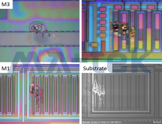
Figure 7 Layer by Layer Delayer Observing the Condition of ESD Circuit Burnout
The important purpose of the ESD failure analysis process mentioned above is to confirm the discharge path. Under this requirement, it is recommended to identify the traces of damage using a Plan View observation method, so that a model of electrostatic discharge failure can be established, and countermeasures for drainage or throttling can be proposed. If it is drainage, it means designing other conduction paths, such as more Contacts to reduce current density. If it is throttling, a current-limiting resistor can be designed to prevent excessive current from causing burning.
Analysis and Solutions for LU Verification Failure
The generation of LU is triggered by external interference signals activating parasitic SCR components, resulting in excessive current that causes functional issues. Therefore, the first step in LU analysis is to identify where the parasitic SCR components are located. When LU occurs, excessive current can potentially cause severe burning of the chip. Although the location of the burn can be easily identified using electrical localization tools, it is important to note that the burn location is the path of high current flow and does not necessarily indicate the location of the parasitic SCR components. Thus, encountering burn phenomena makes it difficult to find the true cause.
When the SCR operates, EMMI can detect the light emitted by the component during operation. Therefore, if the large current caused by the LU phenomenon does not damage the chip, EMMI positioning can be executed under the set conditions that trigger LU, allowing the location of the parasitic SCR component to be identified. Furthermore, the corresponding layout position can be confirmed for the p-n-p-n structure, and this structure can be drawn into a parasitic SCR structure diagram. After that, the principle generated from LU can be used to understand what effect triggered the LU phenomenon, whether it is due to excessive sheet resistance at a certain location, or if there is a floating condition at a certain node, etc. After reasoning out the failure model, the issue of LU can be easily resolved, as referenced in Figure 8.
__26D20oNk2Z.png "8 (2)")
Figure 8: In the CMOS structure, it is necessary to identify the continuity structure of p-n-p-n and correspond it to the SCR circuit.
In the product development stage, ESD and LU testing and analysis are indispensable parts. Following the verification process outlined in this article, certification issues can be resolved quickly. If there are any other special circumstances, please feel free to contact MA-tek's professional team for a more in-depth analysis.


