
Observation of Nano-Dual-Crystal Copper
What is Nano-twin Cu?
Nanotwinned copper refers to the microstructure of copper exhibiting (111) single-direction columnar grains, with high-density twin stacking within the columnar grains, and twin boundary spacing ranging from several nanometers to several hundred nanometers. The nanotwinned copper microstructure with (111) preferred orientation was published by Professor Chen Zhi from the Department of Materials Science and Engineering at National Yang Ming Chiao Tung University in Taiwan in 2012, using special additives in the copper plating solution to deposit copper films through electrochemical plating, forming a patented copper microstructure [1][2]. The structure of the nanotwinned copper is shown in Figure 1. It can be observed in the figure that there is a high density of twin stacking within the copper columnar grains.
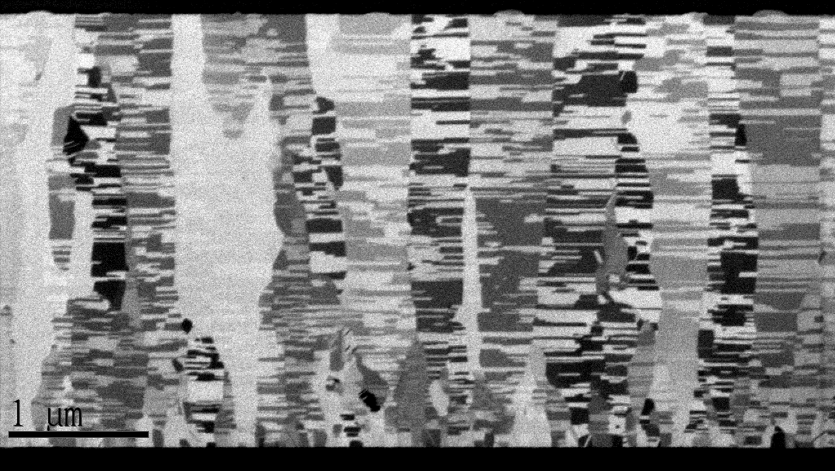
Figure 1 Nanotwinned Copper Structure (Ion-Beam Imaging)
What are the properties of nanocrystalline copper and what is it used for?
The greatest characteristic of nano-twinned copper is the significant improvement in mechanical strength while maintaining similar conductivity. In addition, nano-twinned copper has high thermal stability, excellent resistance to electromigration, and outstanding resistance to the Kirkendall effect. Since Professor Chen Zhi discovered in 2012 that nano-twinned copper can be prepared using direct current electroplating, this technology has been widely researched and utilized.
Moore's Law predicts that the number of transistors per unit area in chips will double every 18 months. This prediction has reached mass production at the 3-nanometer node in 2023, and the development of mass production processes for the 2-nanometer and 1-nanometer nodes is required. The production costs and production technologies have significantly increased, leading experts to predict that Moore's Law will be limited by physical constraints or may be difficult to continue due to cost considerations. Hence, the concept of the post-Moore era (More Than Moore) has emerged. In the post-Moore era, the most notable solutions are Heterogeneous Integration and Chiplet technology. Heterogeneous integration advanced packaging technology has become another important technological development trend for achieving functional integration and component size reduction. This is because heterogeneous integration has driven the development of IC 2.5D and 3D packaging, becoming an inevitable trend, among which the most famous 2.5D/3D packaging technologies include CoWoS (Chip on Wafer on Substrate) and SoIC (System on Integrated Chips), among others.
High-performance copper is needed in many places for connections in 2.5D/3D packaging, including Through-Silicon Via (TSV), bump or micro-bump, Wafer Redistribution Layer (RDL), and Wafer-on-Wafer (WoW). The use of nano-twinned copper in these processes not only enhances the performance at the connection points but also increases the reliability of 2.5D/3D packaging.
Detection of crystallographic orientation
The detection of crystallographic orientation over a large area of the material mainly uses X-ray diffraction analysis (XRD), Electron Back Scatter Diffraction (EBSD), and TEM electron diffraction. XRD has the largest detection range, followed by EBSD, while TEM electron diffraction has the smallest range. TEM electron diffraction will be explained in the next chapter.
The advantage of EBSD is that the grain orientation distribution of the sample surface and cross-section can be confirmed and analyzed. Figure 2 shows the EBSD results of the sample surface, with the Z-axis perpendicular to the sample surface. From the Inverse Pole Figure (IPF), it can be seen that the preferred orientation perpendicular to the sample surface is almost entirely in the 111 direction. Figure 3 shows the EBSD results of the sample cross-section, and from the Inverse Pole Figure, it can be seen that the preferred orientation perpendicular to the sample surface is almost entirely in the 111 direction.
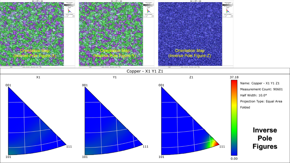
Figure 2 Sample surface EBSD, with the vertical sample surface as the Z-axis. It can be determined from the Inverse Pole Figure that the preferred direction perpendicular to the sample surface is almost entirely along the 111 direction.
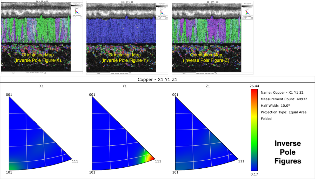
Figure 3 shows the EBSD results of the sample cross-section. From the Inverse Pole Figure, it can be seen that the preferred orientation perpendicular to the sample surface is almost entirely in the 111 direction.
Observation of Nano-twinned Copper
The samples used in this article are all nano-twinned copper samples provided by Professor Chen Zhi from National Yang Ming Chiao Tung University in Taiwan. There are many observation methods for nano-twinned copper, mainly including ion-beam imaging, transmission electron microscopy (TEM), and scanning transmission electron microscopy (STEM), etc.
Ion-beam imaging is the image obtained by irradiating the sample surface with an ion source on a Focus Ion Beam (FIB) microscope, as shown in Figure 1. The ion impacts the sample surface, and due to the differences in the crystallographic orientation of the sample, different channel effects occur, producing different contrasts that can display the nano-twinned structure. In Figure 1, it can be observed that the nano-twins are coated and stacked within the columnar grains. The thickness direction of the nano-twins is approximately the same as the direction of the columnar grains. Comparing with the EBSD results, it can be concluded that the thickness direction of the nano-twins is approximately the same as the length direction of the columnar grains, which is along the copper's 111 crystallographic direction.
TEM uses a 200KV electron beam to penetrate thin samples less than 100nm in thickness to produce thickness contrast or diffraction contrast due to different crystallographic orientations, allowing observation of nanodual-phase copper. In Figure 4, the left image is a TEM bright field image, and the right image is a TEM dark field image. The minimum thickness of the nanodual-phase copper can be measured at approximately 6nm, and the maximum thickness at approximately 125nm. The method of STEM is similar to TEM; STEM irradiates the sample in a scanning manner, as shown in Figure 5. Figure 5 clearly shows the high density of copper twin stacking within the copper columnar grains.
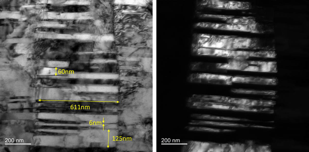
Figure 4 TEM images, the left image is the bright field image, and the right image is the dark field image.
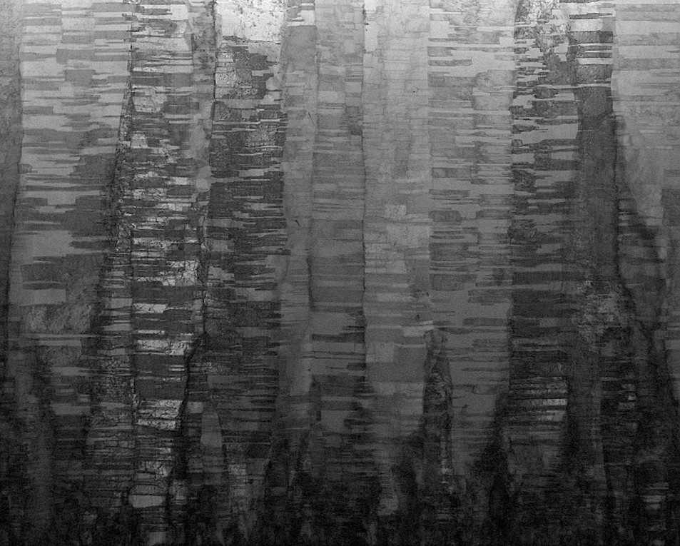
Figure 5 STEM photo, the thickness direction of the nanodual-phase is approximately the same as the length direction of the columnar crystal.
In addition to observing the structure, TEM can also identify the crystallographic direction of grains using electron diffraction techniques. Compared to X-Ray and EBSD, the range of electron diffraction is relatively small, allowing for the identification of the crystallographic direction of individual nanocrystalline grains. Figure 6 shows the electron diffraction pattern of the nanodual-phase copper sample cross-section, which indicates that the results are consistent with EBSD, and the thickness direction of the nanodual-phase is approximately aligned with the length direction of the columnar grains along the copper's (111) crystallographic direction.
In addition to the observation of nano-twinned structures, we can also observe the defect structure of the cross-section. Figure 7 shows the cross-sectional structure of the sample, where longitudinal dislocations can be observed. The longitudinal dislocations are approximately along the 111 direction, and these dislocations are not linear but rather curved and irregular in shape.
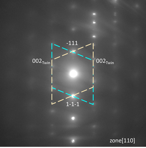
Figure 6 Nanotwinned electron diffraction pattern.
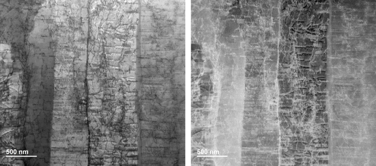
Figure 7 Observing longitudinal dislocations under different STEM conditions.
Nano-twinned copper has become an indispensable technology in advanced packaging such as CoWoS and SoIC in 2.5D/3D packaging since it was proposed by Professor Chen Zhi's team in 2012. A large amount of research and technological development on nano-twinned copper has also driven its increasing applications. The copper interconnection technology required for future advanced packaging technologies such as WoW/RDL/u-bump will inevitably require more nano-twinned copper, so research on nano-twinned copper will only continue to increase. MA-tek has the capability to test nano-twinned copper. This paper uses various methods including EBSD, FIB ion imaging, and TEM/STEM to observe the structure of nano-twinned copper and identify its crystallographic orientation. The results show that the thickness direction of nano-twinned copper is approximately the same as the length direction of the columnar grains, both along the copper's 111 crystallographic direction. In addition, TEM technology can also observe that there are dislocations in the nano-twinned copper that are approximately along the 111 direction, and these dislocations are not linear but exhibit a curved irregular shape.
Reference:
[1] Tianhong Technology, https://www.chemleader.com.tw/autopage_detail/3/nt-cu
[2] HSIANG-YAO HSIAO, CHIEN-MIN LIU, HAN-WEN LIN, TAO-CHI LIU, CHIA-LING LU, YI-SA HUANG, CHIH CHEN , AND K. N. TU,SCIENCE, 25 May 2012, Vol 336, Issue 6084, pp. 1007-1010.
[3] Liu, Tao-Chi, et al. "Fabrication and characterization of (111)-oriented and nanotwinned Cu by DC electrodeposition." Crystal Growth & Design 12.10 (2012): 5012-5016.
[4] Trends in Heterogeneous Integration Advanced Packaging Design, Dr. Hong Zhi-bin - Deputy General Manager of ASE R&D Center


