
Advanced Transistor Technology and Development Trends
Advanced Transistor Technologies and Development Trends
Liu Zhiwei Distinguished/Chair Professor
National Taiwan University Institute of Electrical Engineering
-
With the miniaturization of traditional semiconductor dimensions, the gate length of transistors is also gradually decreasing. To assess semiconductor wafer fabrication technology, the gate width of transistors has traditionally been used as an indicator, as a smaller gate width means a smaller transistor, allowing more transistors to fit on the same size wafer, which in turn implies more functions and better performance. However, in reality, the values of gate length and technology node are not equal, and after the 22-nanometer technology node, the gate length will be greater than the value of the technology node (Figure 1). As the size of transistors continues to shrink, traditional scaling methods are approaching their physical limits. Simply following Moore's Law for size reduction can no longer provide the expected performance growth. Since the 22-nanometer technology node (Intel) and the 16-nanometer technology node (TSMC), the FinFET proposed by Academician Hu Zhengming's team has begun to be adopted by the industry, and three-dimensional transistors have become the mainstream structure of advanced semiconductors today. The current process technology node names conceptually are usually the previous generation process size multiplied by 0.7, representing a halving of the area occupied by transistors, thus doubling the transistor density on the same size wafer. However, with the evolution of the times, simply using gate width can no longer truly assess the performance of the wafer, and the process names of various companies are no longer named after gate width. Therefore, the process sizes frequently mentioned in the news, such as 5 nanometers or 3 nanometers, are more like indicators of advancements in technology nodes and increases in transistor density, rather than actual gate widths. The size of transistors is represented by CPP (Contact Poly Pitch), which is the sum of gate length, 2 spacer (2LSP), and S/D length (Figure 2) [1].
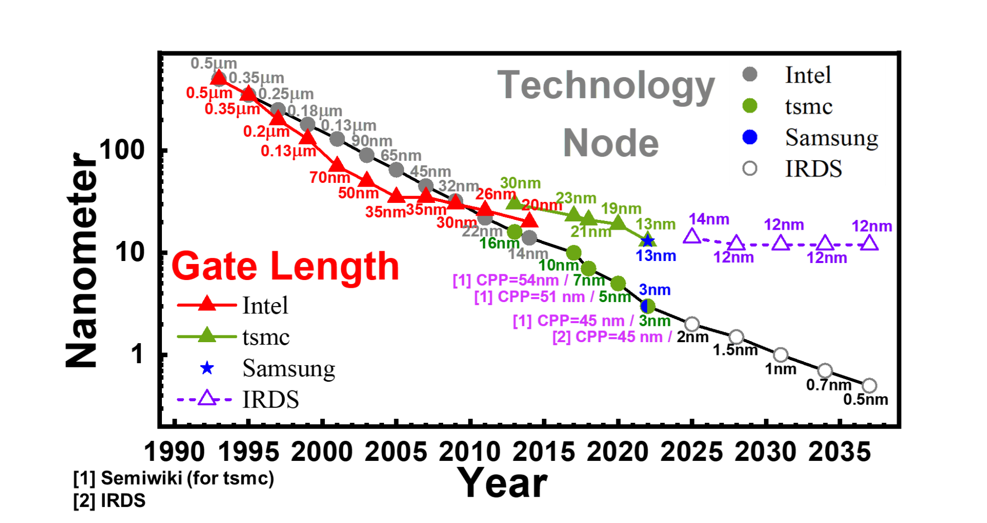
Figure 1: A graph showing the relationship between technology nodes and gate lengths.
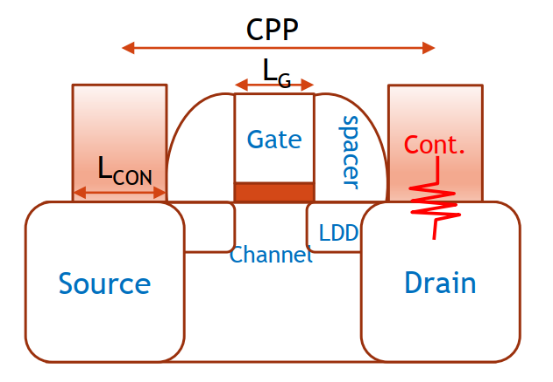
Figure 2: Schematic diagram of transistor CPP (Contact Poly Pitch) [1].
In addition to increasing the drive current of transistors to enhance chip computing performance, reducing power consumption of chips is also a very important direction. Lowering power consumption helps extend the usage time of mobile smart devices and improve device endurance. Among them, the scaling of chip operating voltage (VDD) is an effective method to reduce the power consumption caused by transistor operation. The dynamic power (dynamic power, CVDD2f) generated during transistor operation can be reduced with the scaling of operating voltage; while the current generated when the transistor is in a non-working state is called leakage current (IOFF), the static power (static power, VDDIOFF) caused by leakage current can also be reduced with the decrease of operating voltage. Therefore, with the development of technology nodes, the chip operating voltage must also be scaled (Figure 3). However, after traditional scaling methods, the scaling of operating voltage has already slowed down and even remained at 0.75V. Therefore, the adoption of new technologies to continuously advance the scaling of operating voltage is crucial to achieve lower power consumption. From the current formula, it can be seen that under a fixed ION, if it increases, it can be achieved by high mobility channels, high-κ gate dielectric, and highly stacked channels, then it decreases, that is, VDD can be effectively scaled down, resulting in reduced transistor power consumption (CVDD2f, C is capacitance, f is frequency); additionally, under a fixed ION, if the current switch ratio (ION/IOFF ratio) increases, it can be achieved by ultrathin body, that is, IOFF decreases, resulting in reduced static power (VDDIOFF).
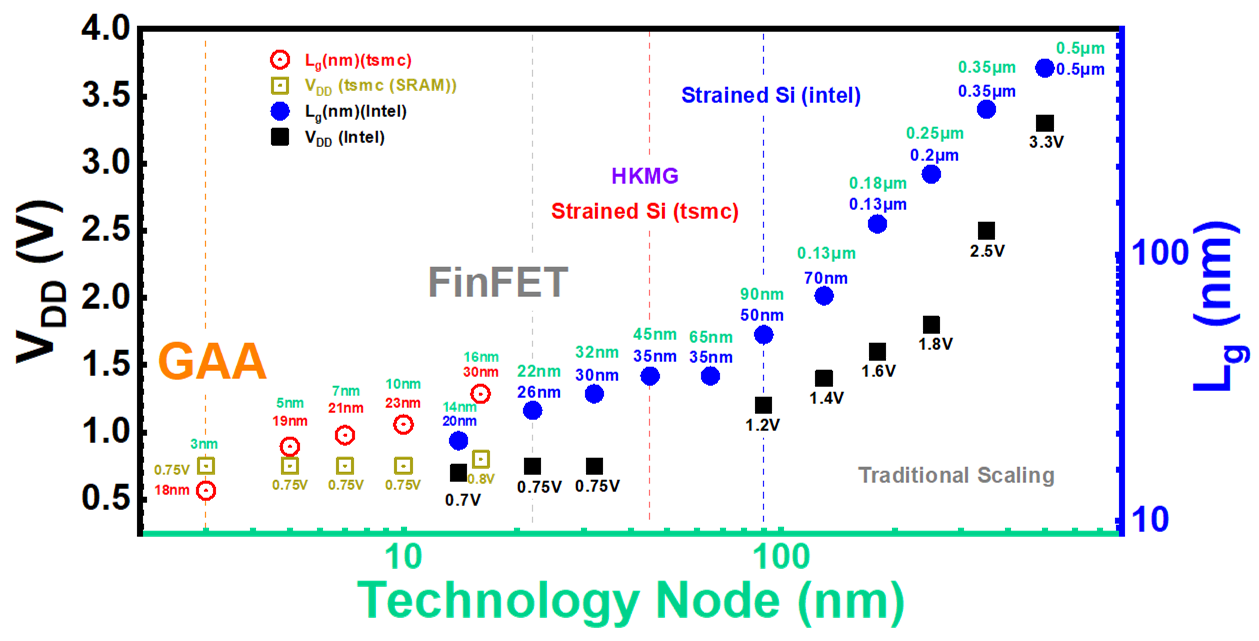
Figure 3: The relationship diagram of working voltage (VDD), gate length (Lg), and technology node.
Starting from the 2-nanometer technology node, the structure of transistors has shifted from FinFET to Gate-All-Around (GAA) stacked nanosheets. GAA transistors have better gate control capabilities than FinFETs, effectively increasing channel control and suppressing short channel effects. According to IMEC's device roadmap (Figure 4) [2], GAA transistors will continue to be used across four technology nodes (N2, A14, A10, A7), and complementary stacked transistors (CFET) will be adopted starting from the A5 technology node. Through the vertical stacking of transistors, the main goal of size reduction is achieved, continuously advancing Moore's Law, with atomic-level channels integrated into CFETs at the A2 technology node. To ensure the continued use of stacked nanosheets, research focuses on advanced nanosheet extensions that integrate new technologies, including channels with high carrier mobility, high-layer stacked channels, and high dielectric constant gate dielectrics. TSMC demonstrated FinFETs with high mobility channels used in the 5-nanometer technology node at the 2019 IEDM [3], with channel materials being silicon-germanium (SiGe) [4], providing higher transistor drive current at the same leakage current compared to silicon channel devices. In terms of stacked channels, Intel's 20A technology node employs four-layer stacked channels of nanoribbons (channel shape similar to nanosheets) [5], while TSMC showcased three-layer stacked channel nanosheets as the transistor structure for the 2-nanometer technology node at the 2021 ISSCC [6]. CEA-Leti demonstrated seven-layer stacked silicon channel nanosheets at the 2020 VLSI [7]. Our research team presented eight-layer stacked Ge0.75Si0.25 nanosheets and seven-layer stacked Ge0.95Si0.05 nanowires at the 2021 VLSI [8], which was selected as the 2021 VLSI Highlight Paper and reported in the prestigious journal Nature Electronics Research Highlight [9].
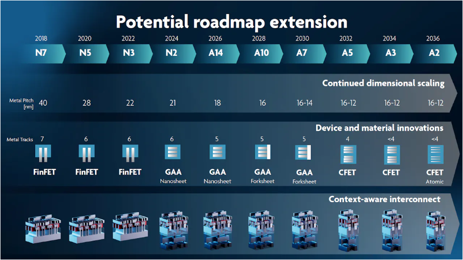
Figure 4: IMEC's transistor structure blueprint [2].
In order to provide greater transistor drive current with the same footprint, the research team continuously increased the number of stacked channels. By optimizing the number of layers of germanium-silicon/ germanium epitaxial layers and using appropriate etching selectivity for isotropic wet etching processes, they successfully fabricated sixteen layers of stacked Ge0.95Si0.05 nanowires (Figure 5 left), which achieved a record drive current (reaching 9400μA/μm per footprint at VOV=VDS=0.5V). To further enhance transistor performance, they successfully fabricated twelve layers of stacked Ge0.95Si0.05 nanowires without parasitic channels (Figure 5 right) using a two-step wet etching process, effectively reducing subthreshold swing (SS) and leakage current. The research results were published in the international journal Nature/Communications Engineering [10]. Currently, National Taiwan University is the only university outside the industry that can conduct long-term research and development of multilayer stacked channel transistors, becoming an important bridge between academia and industry.
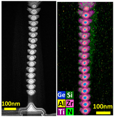
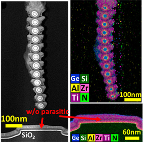
Figure 5: The (left) sixteen-layer stacked Ge0.95Si0.05 nanowires published by this research team. (Right) twelve-layer stacked Ge0.95Si0.05 nanowires without parasitic channels [10].
In order to enhance the drive current of transistors, in addition to increasing the number of stacked layers in the channel, increasing the dielectric constant of the dielectric layers in the gate stack can effectively increase the drive current, while also reducing the number of stacked layers in the channel to lower the difficulty of the manufacturing process. By using plasma-enhanced atomic layer deposition (PEALD) HfxZryO2 dielectric layers, and optimizing the concentrations of Hf and Zr to achieve a high dielectric constant, our research team successfully integrated Hf0.2Zr0.8O2 high dielectric constant (κ=47) dielectric layers into eight-layer stacked Ge0.95Si0.05 nanowires (left in Figure 6) and nanosheets (right in Figure 6), with the research results published in 2023 VLSI [11]. Nanowires and nanosheets exhibited drive currents of 9200μA/μm per footprint and 360μA per stack, respectively, at VOV=VDS=0.5V (with nanosheets achieving a record drive current). Furthermore, simulations confirmed that HZO with [Zr]=80% can achieve a peak dielectric constant, and simulations validated that high dielectric constant gate stacks combined with high-layer stacked channels can effectively reduce gate delay.
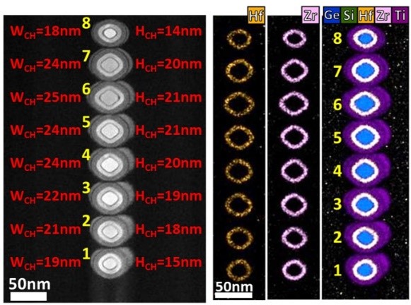
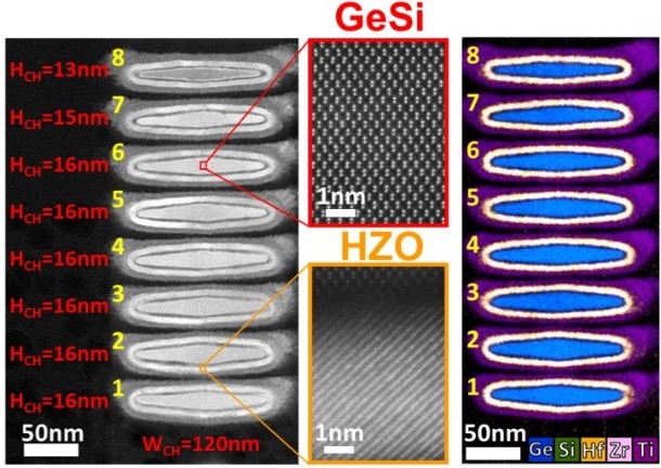
Figure 6: The research team published the integration of Hf0.2Zr0.8O2 high-k dielectric layer on (left) eight-layer stacked Ge0.95Si0.05 nanowires. (right) eight-layer stacked Ge0.95Si0.05 nanosheets [11]. ©2023 JSAP
Germanium-silicon (GeSi), germanium (Ge), and germanium-tin (GeSn) based materials have a higher carrier mobility than silicon, which can increase the drive current of transistors, and they are compatible with current silicon semiconductor process technologies, showing potential to become the next generation channel materials. Other novel non-silicon based materials, such as oxide semiconductors and two-dimensional materials (2D materials) for use as transistor channels, have been widely researched in recent years. Among them, due to the characteristics of monolayer atoms, many people have high hopes for the scaling potential of two-dimensional materials, with relevant papers discussed in Nature, IEDM, and VLSI. However, two-dimensional materials face challenges in large-area high-quality wafer growth technology, as well as issues such as high contact resistance and low current. In terms of device processing, two-dimensional materials are difficult to integrate with mature silicon-based materials in the industry, and their performance is also inferior compared to group IV material transistors. For n-type transistors, most oxide semiconductors and two-dimensional material transistors exhibit negative threshold voltage (VT) and relatively large overdrive voltage (VOV) (Figure 7 above) [12], making them unsuitable for advanced IC applications. Additionally, for p-type transistors, most oxide semiconductors and two-dimensional material transistors still show relatively large VOV, making them similarly unsuitable for advanced IC applications (Figure 7 below). Compared to oxide semiconductors and two-dimensional materials, high carrier mobility group IV materials can still achieve higher drive currents under low VOV conditions.
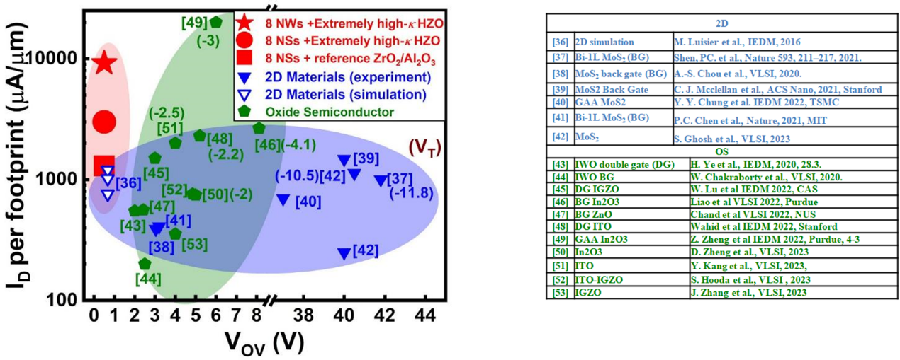
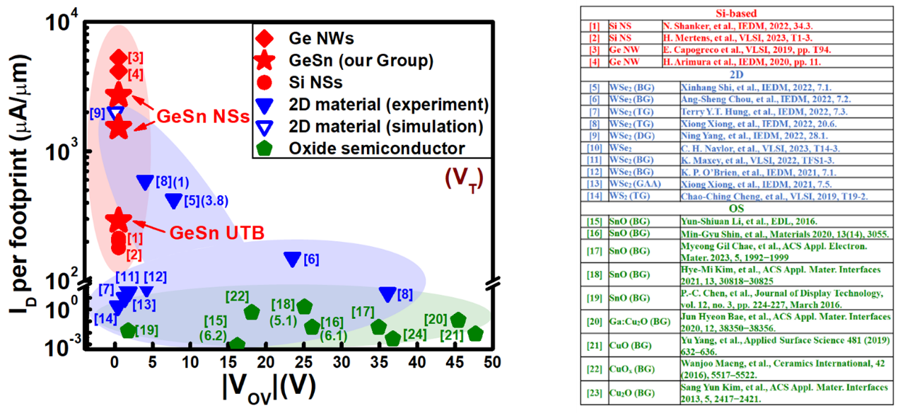
Figure 7: Comparison of current and VOV for (top) n-type transistors of four types of materials, oxide semiconductors, and two-dimensional materials [12] © IEEE and (bottom) p-type transistors.
According to IMEC's component blueprint (Figure 4) [2], complementary stacked transistors (CFET) will be introduced at the A5 technology node (2032). Compared to horizontally placed transistors, complementary stacked transistors can reduce the footprint of inverter cells, potentially shrinking the area of inverter cells by half (Figure 8) [4], thereby increasing the number of transistors per unit area and enhancing computational performance. This continues to advance technology nodes and has become an important topic of research. The industry is also actively developing complementary stacked transistors in preparation for the next transistor architecture to replace stacked nanosheets. At the 2023 IEDM, Intel (Figure 9 upper left) [13], Samsung (Figure 9 upper right) [14], and TSMC (Figure 9 lower) [15] all presented research and development results on complementary stacked transistors.
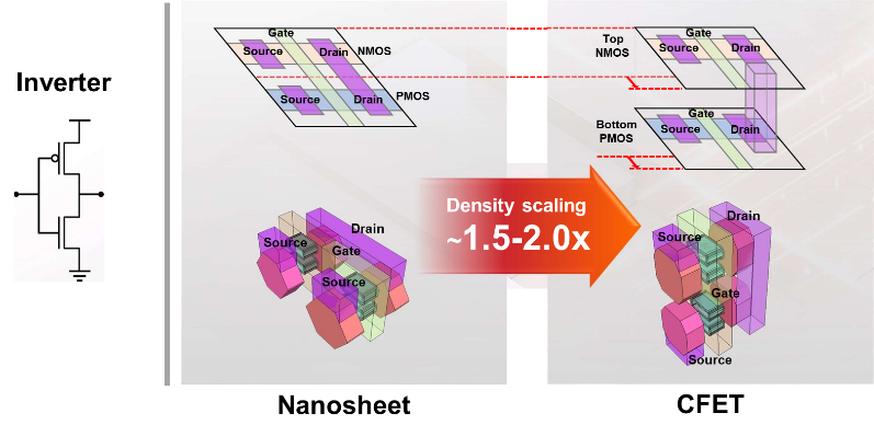
Figure 8: Schematic diagram of complementary stacked transistors, further reducing the footprint of the inverter unit (up to half of the original area). [4]
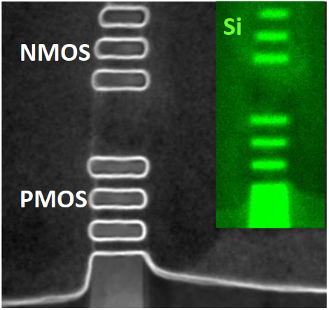
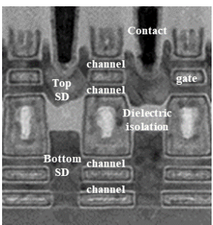
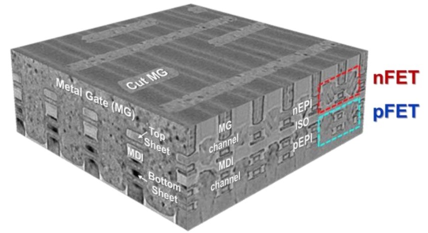
Figure 9:
(Top left) Complementary stacked transistors presented by Intel [13]. © IEEE
(Upper right) Complementary stacked transistors announced by Samsung [14]. © IEEE
(Below) TSMC's announcement of complementary stacked transistors [15]. © IEEE
This research team has successfully developed a complementary stacked transistor structure for the 0.5nm (5Å) generation, stacking n-type and p-type nanosheet transistors in the vertical direction (Figure 10) and successfully measuring the inverter characteristics of the inverter structure. By using three-dimensional monolithic stacking, the channel layer of the bottom transistor, the intermediate sacrificial layer, and the channel layer of the upper transistor are grown epitaxially without the need for wafer bonding technology, which simplifies process complexity and reduces wafer costs. High mobility germanium-silicon channels are used as n-type and p-type nanosheets in the complementary stacked transistors to improve performance. In the stacked transistor structure, good isolation between transistors is essential to ensure that each transistor can operate independently without mutual interference. This research team employs multilayer P/N junctions as electrical isolation between stacked transistors, eliminating the need for complex source/drain regrowth processes and effectively replacing insulation layer deposition to simplify the device fabrication process. Relevant results have been published in the 2022 IEDM International Conference [16].
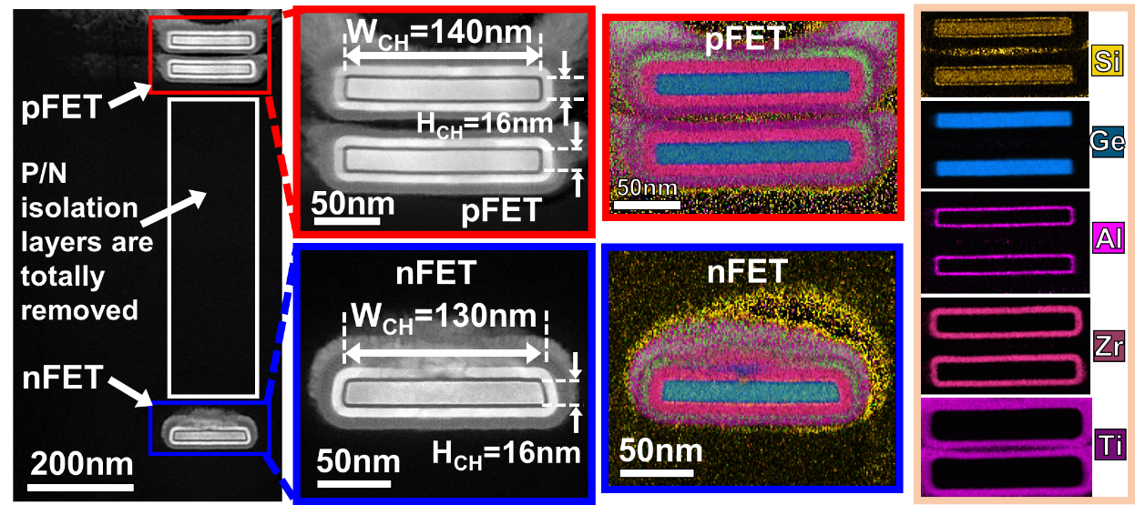
Figure 10: The complementary stacked transistor with germanium-silicon channels published by this research team consists of vertically stacked p-type nanosheet transistors on top of n-type nanosheet transistors to form an inverter unit [16]. © IEEE
Based on the development experience of single-chip complementary stacked transistor structures, this research team further optimized the process to achieve the world's first single-chip stacked integrated complementary stacked transistors of heterogeneous germanium-tin and germanium-silicon nanosheets (Figure 11). By epitaxially growing the channel layer of the bottom germanium-silicon nanosheet transistors, the sacrificial layer in the middle, and the channel layer of the upper germanium-tin nanosheet transistors, the integration of heterogeneous germanium-tin and germanium-silicon channels can be achieved without wafer bonding. Furthermore, through the band alignment between the germanium-tin and germanium-silicon channels, an inverter with VT matching is completed using only a single type of metal work function gate stack (Figure 12), eliminating the need for the complex process of high aspect ratio dual metal work function gate stacking. The complementary stacked transistors of heterogeneous germanium-tin and germanium-silicon channels can have better inverter characteristics compared to the VT mismatched germanium-silicon channel complementary stacked transistors. In addition, a high dielectric constant Hf0.2Zr0.8O2 gate dielectric layer is integrated, which can effectively enhance the performance of the complementary stacked transistors. Relevant results have been published in the 2023 IEDM International Symposium [17].
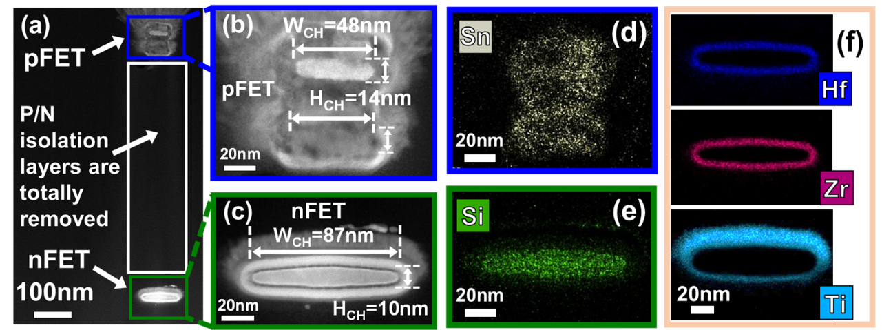
Figure 11: The research team published a complementary stacked transistor with heterogeneous germanium-tin and germanium-silicon channels, successfully stacking p-type germanium-tin nanosheets vertically on top of n-type germanium-silicon nanosheets to form an inverter unit [17]. © IEEE
Figure 12: The inverter with VT matching can be completed through the band offset between the heterojunction germanium-tin and germanium-silicon channels [17]. © IEEE
According to the current research and development status, two-dimensional materials need a lot of effort to replace silicon-based materials and become mainstream technology.
Reference:
[1] Jin Cai, "CMOS Device Technology For the Next Decade," IEEE Symposia on VLSI Technology and Circuits (VLSI), SC1-1, 2021.
[2] "20-year semiconductor roadmap" [Online] https://www.imec-int.com/en/articles/20-year-roadmap-tearing-down-walls
[3] G. Yeap et al., "5nm CMOS Production Technology Platform featuring full-fledged EUV, and High Mobility Channel FinFETs with densest 0.021μm2 SRAM cells for Mobile SoC and High Performance Computing Applications," IEEE International Electron Devices Meeting (IEDM), pp. 879-882, 2019.
[4] Y. -J. Mii, "Semiconductor Innovations, from Device to System," 2022 IEEE Symposium on VLSI Technology and Circuits (VLSI Technology and Circuits), 2022, pp. 276-281.
[5] “Intel Accelerated” [Online] https://download.intel.com/newsroom/2021/client-computing/Intel-Accelerated-2021-presentation.pdf
[6] Mark Liu, "Unleashing the Future of Innovation," 2021 IEEE International Solid-State Circuits Conference (ISSCC), Plenary Session 1.1, 2021.
[7] S. Barraud et al., "7-Levels-Stacked Nanosheet GAA Transistors for High Performance Computing," IEEE Symposia on VLSI Technology and Circuits (VLSI), TC1.2, 2020.
[8] Y.-C. Liu et al., "First Highly Stacked Ge0.95Si0.05 nGAAFETs with Record ION = 110 μA (4100 μA/μm) at VOV=VDS=0.5V and High Gm,max = 340 μS (13000 μS/μm) at VDS=0.5V by Wet Etching," IEEE Symposia on VLSI Technology and Circuits (VLSI), T15-2, 2021.
[9] S. Thomas, “Germanium nanowire transistors stack up,” Nature Electronics, Vol. 4, July 2021, 452.
[10] Y.-R. Chen et al., "Fabrication and performance of highly stacked GeSi nanowire field effect transistors," Communications Engineering, 2, 77, 2023.
[11] Y.-C. Liu et al., "Extremely High-κ Hf0.2Zr0.8O2 Gate Stacks Integrated into Ge0.95Si0.05 Nanowire and Nanosheet nFETs Featuring Respective Record ION per Footprint of 9200μA/μm and Record ION per Stack of 360μA at VOV=VDS=0.5V," IEEE Symposia on VLSI Technology and Circuits (VLSI), T16-4, 2023.
[12] W.-J. Chen et al., "Extremely High-κ Hf0.2Zr0.8O2 Gate Stacks Integrated Into Eight Stacked Ge0.95Si0.05 Nanowires and Nanosheets nFETs to Boost ION," IEEE Transactions on Electron Devices, 70, 12, 2023.
[13] M. Radosavljević et al., “Demonstration of a Stacked CMOS Inverter at 60nm Gate Pitch with Power Via and Direct Backside Device Contacts,” IEEE International Electron Devices Meeting (IEDM), 29-2, 2023.
[14] J. Park et al., "First demonstration of 3-dimensional stacked FET with top/bottom source-drain isolation and stacked n/p metal gate," IEEE International Electron Devices Meeting (IEDM), 29-4, 2023.
[15] S. Liao et al., "Complementary Field-Effect Transistor (CFET) Demonstration at 48nm Gate Pitch for Future Logic Technology Scaling," IEEE International Electron Devices Meeting (IEDM), 29-6, 2023.
[16] C.-T. Tu et al., "First Demonstration of Monolithic 3D Self-aligned GeSi Channel and Common Gate Complementary FETs by CVD Epitaxy Using Multiple P/N Junction Isolation," IEEE International Electron Devices Meeting (IEDM), pp.479-482, 2022.
[17] C.-T. Tu et al., "First Demonstration of Monolithic Self-aligned Heterogeneous Nanosheet Channel Complementary FETs with Matched VT by Band Alignments of Individual Channels," IEEE International Electron Devices Meeting (IEDM), 29-5, 2023.


