
Circuit Repair Technology Solutions and Processes
In the IC design and manufacturing process, products that undergo tape-out after R&D need to undergo functional verification to confirm whether they meet testing standards. However, there often exist performance differences and even functional defects, which necessitate design debugging to identify issues and revise the design for re-manufacturing. This entire process forms a loop; the faster the issues are identified, the quicker the product can be brought to market. As products become increasingly complex, the time taken to revise new photomasks, manufacture, and produce a finished product is very time-consuming. If the time spent on design debugging can be reduced, it can shorten the overall time from engineering to mass production. There are many methods for design debugging, including testing, simulation, failure analysis, and circuit repair. The engineering team invests considerable effort in identifying issues to ensure that the next revision of the product can achieve the desired performance. Among these methods, circuit repair is one that almost all R&D engineers utilize. By modifying the circuit, the need to redo photomasks and the initial prototype R&D costs can be eliminated. This operational model is absolutely effective in shortening the time from R&D to mass production while also saving a significant amount of R&D expenses, making the client's products more timely and competitive in R&D. This article describes the principles and considerations of circuit repair, facilitating effective and efficient communication between R&D engineers and integration engineers when requesting circuit repair.
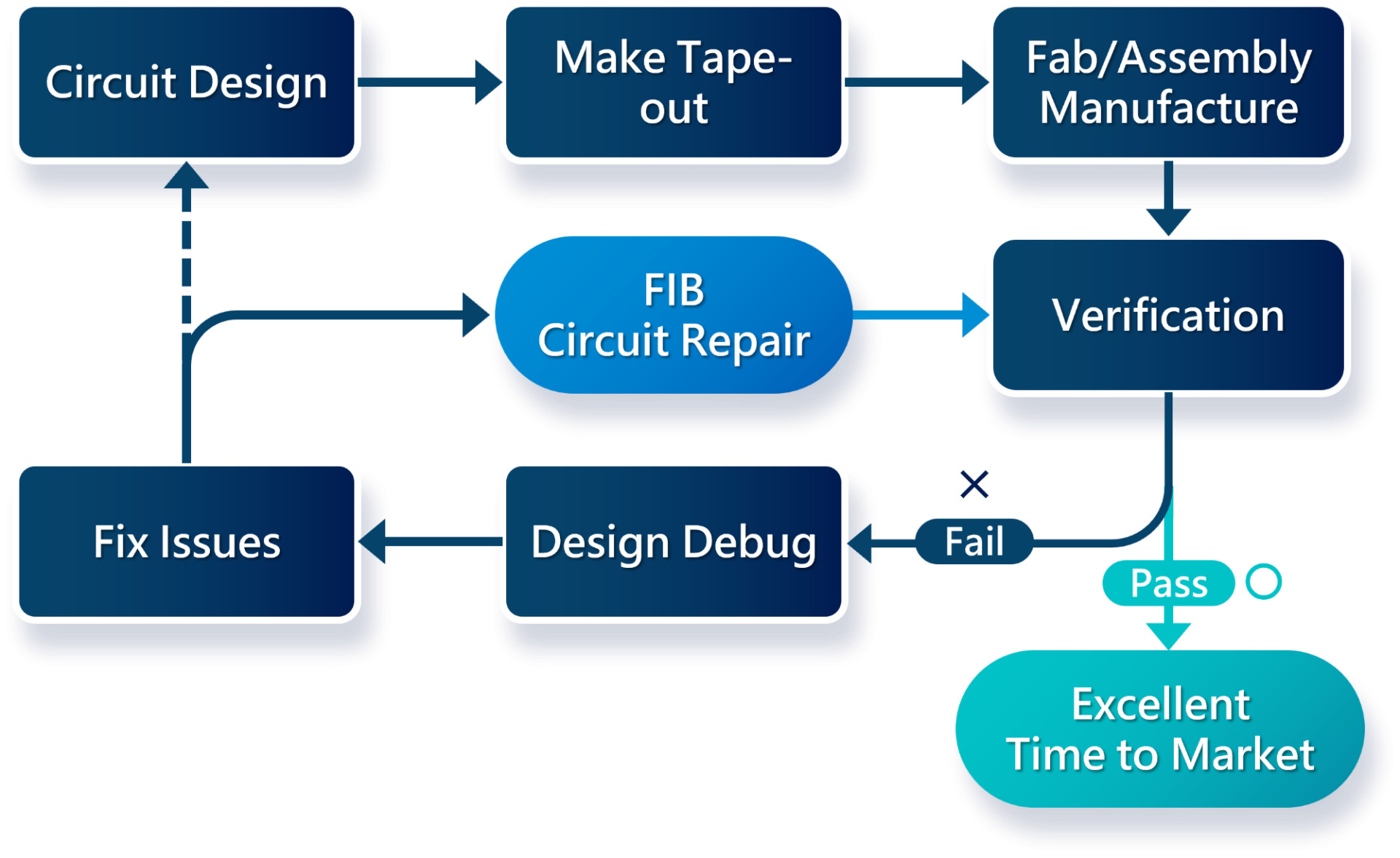
Figure 1 is a flowchart from circuit design, product manufacturing, verification, identifying design issues to revisions. The faster the problems are solved, the shorter the time to market, gaining a competitive advantage.
FIB circuit repair, also known as circuit edit, commonly abbreviated as FIB, is a type of instrument developed for modifying the layout on ICs. FIB machines have many functions, including localized cross-sectional observation and TEM sample preparation for structural or failure analysis. To avoid confusion, it is still recommended to specify that circuit repair will be performed during the commissioning, rather than just saying FIB. The type of machine used for circuit repair belongs to single beam, meaning it uses an ion beam for ion impact to remove surface material as a tool for circuit cutting. If circuit connections are to be made, a metal layer, such as tungsten, must be deposited to connect two or more metal lines. At this time, it is also necessary to use W(CO)6 gas, which, after being decomposed by the Ga+ ion beam, can achieve the tungsten coating (Figure 2).
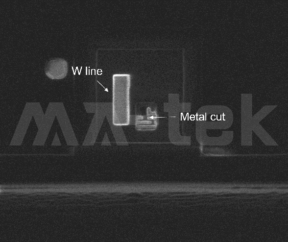
Figure 2 Scheme 1 line 1 cut represents the cutting of one metal line and the connection of two metal lines, with the metal material for the connection being tungsten.
The process of circuit repair will first involve internal discussions on the client side to identify the locations that need modification, followed by providing a proposal and process. The proposal includes the planar positions and metal layers for the required circuit cutting and connections, and it is determined whether the client needs to provide GDS files based on the situation. Generally, if the circuit cannot be clearly identified from the surface of the sample, GDS is needed for automatic navigation to the correct position to reduce the failure rate of execution (Figure 3). Considering cybersecurity risks, regional GDS files can be provided (Figure 4). After the sample is completed, if there are no further requirements, the executing unit will delete the files. After receiving the request, the executing unit needs to discuss and evaluate the case with the commissioning client, providing the required man-hours and proposal yield. If necessary, the proposal can be modified to improve the success rate of the execution. Once both parties confirm that there are no issues, it will enter the execution schedule, and upon completion, it will be sent back to the client for testing to verify whether the proposal is successful.
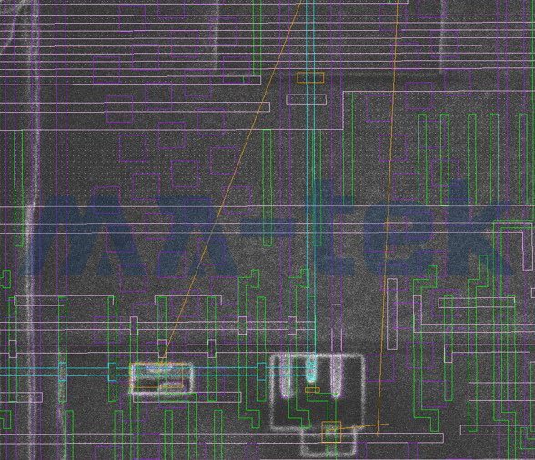
After aligning the GDS layout in Figure 3 with the sample surface, the correct position for circuit repair is found using coordinates.
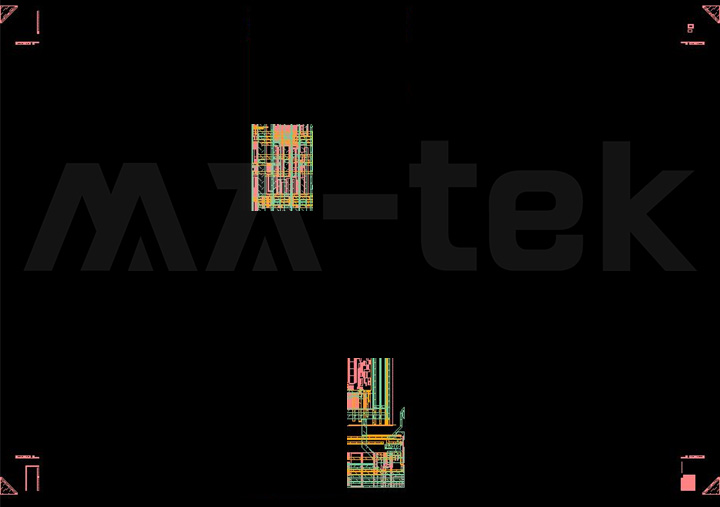
Figure 4 The GDS provided by the customer must include the positions of the four corners for calibration, as well as the GDS for the location and layers of circuit repair, without disclosing customer confidential information.
The time and yield required for executing circuit repair will vary depending on the sample's process, the difficulty of the solution, and the completeness of the sample information. The methods and techniques used must be adjusted in real-time according to the current execution situation. Therefore, it relies not only on advanced instruments and devices but also requires engineers with considerable experience to face and resolve various unexpected situations, thereby achieving the results expected by the customers.
Currently, in addition to the general circuit repair from the front side of the IC, the changes in current processes and packaging technologies also provide the following services:
1. Backside CKT analysis service: For flip-chip packaging, circuit repair needs to be performed from the back of the IC chip. Currently, most samples are from the 5nm to 28nm process. In this regard, MA-tek is equipped with the latest Centrios machines, and the engineers have comprehensive qualifications, achieving an overall yield of over 90% (Figure 5).
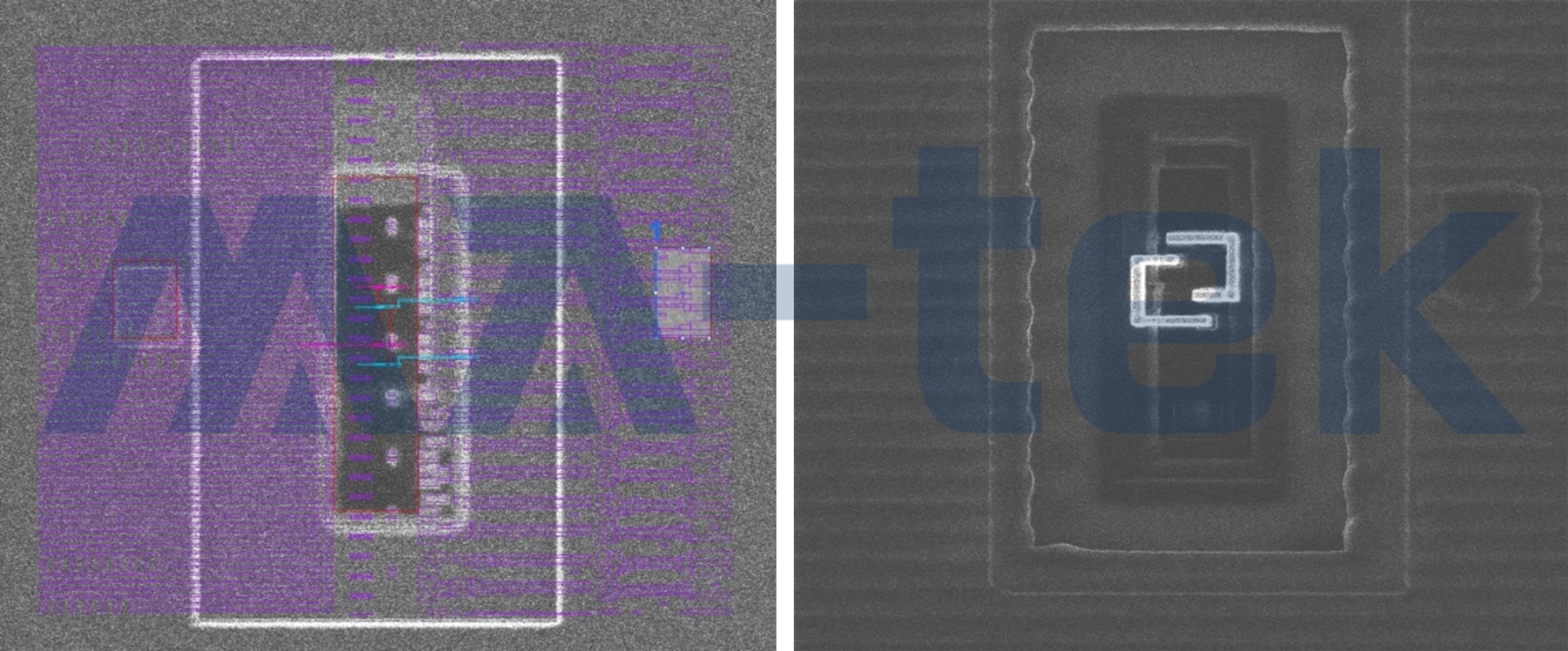
Figure 5 Backside Circuit Repair Example
2. N-wire external leads: For signals that need to be measured, the signals are routed to the surface of the IC through circuit editing, and then connected to the IC pins with regular solder wires. This allows for dynamic measurements on the machine, which is more flexible compared to the traditional method of observing the oscilloscope after creating cross pressure points (PAD) and using probing (Figure 6).
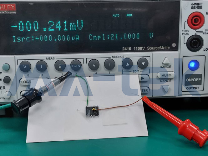
Figure 6 N-wire can bring internal signals of the chip out for measurement.
3. CSP ball removal and re-ball service: If the position that needs circuit repair is below the solder ball, the solder ball can be removed for execution, and after completion, the solder ball can be re-balled without affecting subsequent testing (Figure 7).
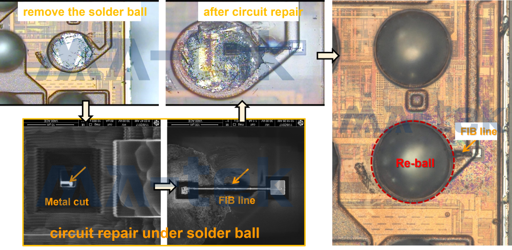
Figure 7 Photos of each stage of circuit repair under solder balls
As the technology becomes more advanced, the difficulty of circuit repair is also increasing, making the maintenance and improvement of yield a critical factor and an essential means of maintaining customer relationships. Therefore, MA-tek spares no effort in investing in equipment and training talent. Internal skill upgrades and education training are continuously carried out according to established processes and schedules, progressing together with the entire semiconductor industry to achieve precision and accuracy, efficiency and effectiveness! Just like MA-tek's original entrepreneurial intention, The Best R&D Partner!


