
Research on the characteristics of N-type β-Ga2O3 polycrystalline films grown on sapphire substrates by ion implantation and their device properties.
N-type β-Ga2O3 polycrystalline films grown on sapphire substrates by ion implantation and
Research on its device characteristics
Professor Hong Ruihua
Tsai Hsin-Ying, Aproova Sood (PhD students)
National Yang Ming Chiao Tung University Institute of Electronics
-
Currently, the semiconductor industry mainly uses Si to manufacture various devices. However, with the advancement of process technology and improvements in device structures, the related devices made from Si have reached the limits of material properties. As technology develops, whether it is the demand for communication in 5G and 6G, the requirements of the green energy industry, or the development of electric vehicles, the devices used are all moving towards the demands for higher speed or higher power. These device characteristics are beyond what Si devices can achieve, thus it is necessary to use other semiconductor materials to meet the characteristics of high-speed or high-power devices.
In recent years, the rapid development of electric vehicles and renewable energy has led to an increasing demand and performance requirements for power devices. However, the bandgap (Eg) of Si is only 1.12 eV, which cannot withstand high voltages. Currently, high-voltage and high-power power devices are gradually adopting third-generation wide bandgap semiconductors such as silicon carbide (SiC) and gallium nitride (GaN). Devices made from these materials can significantly enhance the voltage and power of power devices, thereby improving conversion efficiency in applications related to electric vehicles and renewable energy.
Baliga's Figure-Of-Merits (BFOM) is commonly used to evaluate the characteristics of semiconductor materials in power devices. BFOM is proportional to εμEc3. As the energy gap (Eg) of the material increases, the critical electric field (Ec) of the material also increases, leading to a significant increase in BFOM. A larger BFOM indicates a higher potential of the material in power devices. As shown in Table 1, the Eg of SiC and GaN are 3.3 and 3.4 eV, respectively, resulting in BFOM values of 340 and 870 compared to Si. However, the growth conditions for native substrates of SiC and GaN are stringent and expensive, making the power devices produced much more costly than Si MOSFETs and Si IGBTs. On the other hand, the growth conditions for the fourth-generation wide bandgap oxide semiconductor Ga2O3 do not require high temperature and pressure, resulting in lower costs. Moreover, Ga2O3 has an Eg of up to 4.8 eV, with BFOM values that are 4 times and 10 times that of SiC and GaN, respectively. If power devices can be successfully fabricated, it can effectively increase the breakdown voltage of the devices. Additionally, the on-resistance of devices made from this material is theoretically lower than that of Si, GaAs, SiC, and GaN. Lower on-resistance can reduce power consumption during device operation, thereby improving conversion efficiency. Therefore, Ga2O3 is seen as a potential replacement for SiC and GaN, becoming the semiconductor material for the next generation of high-power devices. Some even suggest that Ga2O3 may replace SiC applications within the next decade.
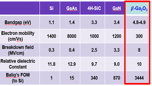
Figure 1 Comparison of Semiconductor Material Properties
Ga2O3 has a total of five crystal phases (Polymorphs): monoclinic (β-Ga2O3), rhombohedral (α-Ga2O3), defective spinel (γ-Ga2O3), cubic (δ-Ga2O3), and orthorhombic (ε-Ga2O3). Among them, β-Ga2O3 has the highest stability, while the other four crystal phases will all transform into β-Ga2O3 at high temperatures. β-Ga2O3 has high chemical stability and thermal stability, and possesses a bandgap of up to 4.8 eV, making it very suitable for power devices.
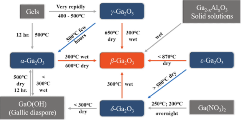
Figure 2. Relationship diagram of various Ga2O3 crystal phase transitions [1]
Despite the many advantages of β-Ga2O3, it is necessary to have a film with controllable conductivity to fabricate devices. Due to the high energy gap of β-Ga2O3, which reaches 4.8 eV, its intrinsic carrier concentration is only 1.79 × 10⁻²³ cm-3, resulting in an extremely high resistivity for undoped β-Ga2O3, making it behave like an insulator and unsuitable for semiconductor device fabrication. Due to the properties of the material, it is currently very difficult to prepare P-type β-Ga2O3, whereas there is still a chance to achieve N-type β-Ga2O3. According to theoretical calculations, the donor levels of impurities such as Si, Ge, and Sn in β-Ga2O3 are very close to the conduction band, with activation energies of 30, 30, and 60 meV, respectively, indicating shallow donor levels. Experiments have demonstrated that the activation rates of these impurities are high. Several research teams have previously used molecular beam epitaxy (MBE) to grow β-Ga2O3 on β-Ga2O3 substrates, doping with Si, Ge, and Sn, which can effectively enhance the electron concentration of β-Ga2O3 and reduce the sheet resistivity of β-Ga2O3, making it suitable for power device fabrication.
MBE devices require ultra-high vacuum, and their deposition rate is slow and cost is high, making them unsuitable for mass production, only suitable for early research and verification of materials. Metal-organic Chemical Vapor Deposition (MOCVD) has high yield, lower cost, and good crystallinity, making it suitable for mass production of β-Ga2O3. Zixuan Feng and his team used a MOCVD system to introduce Triethylgallium (TEGa) and O2, and used Silane (SiH4) as a precursor to prepare in-situ Si doped β-Ga2O3 films. They can also change the chamber pressure to control the Si doping concentration. Through Hall measurement, the carrier concentration can reach over 10^16 cm-3, and the carrier mobility at room temperature can reach 184 cm2/V·s.
Although our research team has successfully developed polycrystalline β-Ga2O3 films on β-Ga2O3 substrates, β-Ga2O3 substrates are still not widely used and remain high-priced materials. In contrast, the c-plane Sapphire substrate, which has a lattice constant very close to that of β-Ga2O3, is much more affordable and has greater market competitiveness. Our laboratory has been able to grow high-quality undoped (UID) (-2 0 1) β-Ga2O3 on c-plane Sapphire substrates using MOCVD. XRD measurements show that the full width at half maximum (FWHM) of the (-2 0 1) peak can be as low as 400 arcsec, indicating that this β-Ga2O3 has a high degree of crystallinity.
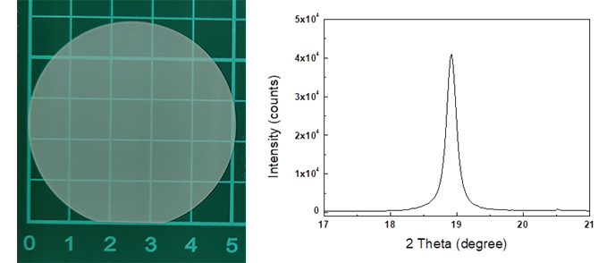
Figure 3. (a) Wafer diagram of β-Ga2O3 on Sapphire (b) XRD diagram
In order to enhance the conductivity of UID β-Ga2O3, we used Si ion implantation technology to implant Si into the β-Ga2O3 film, and employed rapid thermal annealing (RTA) at high temperatures to repair the defects caused by Si ion collisions and activate the Si dopant. By varying the implantation dose and energy of Si implantation, the concentration distribution of Si can be altered, and combined with photolithography, doping can be performed in specific areas. Compared to adding dopants during polycrystalline growth, ion implantation provides greater flexibility in modifying the electrical properties of the polycrystalline film in device fabrication.
On the other hand, the Schottky barrier diode (SBD) is a common power device. The SBD achieves rectification characteristics through the Schottky junction between metal and semiconductor. The SBD has characteristics such as low forward voltage, high forward current, and high switching speed. In research, the SBD can extract the carrier concentration of the semiconductor using I-V and C-V methods, and can also determine the breakdown voltage, material stability, and quality of the semiconductor through temperature variation and high voltage measurements. Therefore, this paper will evaluate the feasibility of producing high-power SBDs using doped SBDs grown heterogeneously on Sapphire Ga2O3.
We used three Si implantation doses to inject into β-Ga2O3 polycrystalline films, namely 1x10^14, 6x10^14, and 1x10^15 cm-2, followed by high-temperature RTA treatment to activate the Si dopant. Since Si implantation requires high-energy Si ions to impact the surface of β-Ga2O3 to implant into the polycrystalline film, it is easy to generate defects on the surface of the samples. Therefore, we conducted atomic force microscopy (AFM) measurements on these three Si implanted samples and UID β-Ga2O3, and the results are shown in Figure 4. Compared to UID β-Ga2O3, after Si implantation, Si fills Ga vacancies, resulting in a reduction of defects, thus the root mean square (RMS) roughness of Si implanted β-Ga2O3 decreases. As the implantation dose increases, Si atoms form complexes, leading to defect accumulation and an increase in surface roughness.
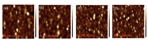
Figure 4. (a) AFM image of UID β-Ga2O3 SBD; AFM images for Si implantation doses of (b) 1x10^14 cm-2 (c) 6x10^14 cm-2 (d) 1x10^15 cm-2.
In order to further the research, we fabricated SBDs using three doses (1x10¹⁴, 6x10¹⁴, 1x1015 cm-2) of Si Implantation β-Ga2O3 and compared them with UID β-Ga2O3 SBDs. For the fabrication of SBDs, the anode electrode used Ni/Au as the Schottky contact, and the cathode electrode used Ti/Au/Ti/Al as the Ohmic contact. The cross-sectional structure diagram of the devices and the electrode patterns were observed using scanning electron microscopy (SEM), as shown in Figure 5.
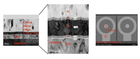
Figure 5. Cross-section and top view SEM images of β-Ga2O3 SBD.
After the β-Ga2O3 SBD was completed, I-V measurement analysis was conducted using the Keysight B1505A power device analyzer, with results shown in Figure 6. After Si implantation, the on-state current of the SBD can be increased by 108 times, and as the Si implantation dose increases, the current increases significantly, indicating that Si replaces Ga to provide electrons, increasing the carrier concentration, effectively reducing the resistance of β-Ga2O3 and enhancing the performance of the device. The J-V curve was differentiated to calculate Ron,sp, with results shown in Figure 7. The Ron,sp of the SBD after Si implantation decreased significantly. Fitting analysis was performed on the J-V curve using Equation 1 to calculate the ideality factor (Ideality Factor, η) of the SBD. The closer the η value is to 1, the more the device characteristics approach the ideal formula. The η of the UID β-Ga2O3 SBD is 8.05. The SBD after Si implantation effectively reduces the series resistance, thus significantly lowering the η value. As the implantation dose increases, η rises from 1.37 to 2.08 due to the increase in doping concentration (ND), leading to tunneling effects, which causes the η value to rise.
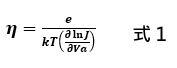
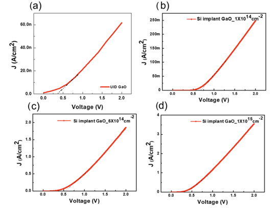
Figure 6. (a) I-V curve of UID β-Ga2O3 SBD; I-V curves for Si implantation doses of (b) 1x10^14 cm-2 (c) 6x10^14 cm-2 (d) 1x10^15 cm-2
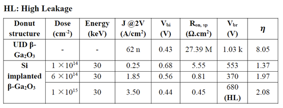
Figure 7. Characteristics table of UID and Si Implantation β-Ga2O3 SBD
The C-V measurement results of β-Ga2O3 SBD are shown in Figure 8. Using semiconductor device physics formulas (Equations 2 to 7) for analysis, the carrier concentrations of Si Implantation β-Ga2O3 at three doses (1x10^14, 6x10^14, 1x10^15 cm-2) were calculated to be 1.08x10^17, 4.31x10^18, and 1.07x10^19 cm-3, respectively, indicating that Si Implantation technology can significantly adjust the carrier concentration and conductivity of β-Ga2O3. The UID β-Ga2O3 SBD, however, had a resistance that was too high, exceeding the machine's analytical limit. By substituting the calculation results of Equations 3 to 7 into Equation 2, the Effective Schottky Barrier Height (ϕBn) can be calculated. The ϕBn values for the three doses (1x10^14, 6x10^14, 1x10^15 cm-2) of Si Implantation β-Ga2O3 are 0.82, 0.54, and 0.32V, respectively. As the implantation dose increases, the Metal Induced Gap States (MIGS) cause more severe Fermi level pinning, resulting in a decrease in ϕBn and an increase in reverse leakage current.
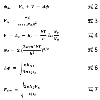
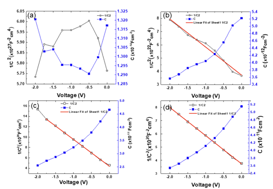
Figure 8. (a) C-V curve of UID β-Ga2O3 SBD; C-V curves for Si implantation doses of (b) 1x10^14 cm-2 (c) 6x10^14 cm-2 (d) 1x10^15 cm-2
As high-voltage, high-power devices, β-Ga2O3 SBDs need to withstand high reverse bias voltages. Therefore, we conducted breakdown measurements at high voltages on these four devices. The breakdown voltage (VBD) of the UID β-Ga2O3 SBD reached as high as 1030 V. However, as the Si implantation dose increased, VBD decreased, indicating that a large number of defects were generated after high-dose implantation. Therefore, further treatment and analysis are needed after implantation to reduce defect density, lower the reverse leakage current of the SBD, and enhance VBD.
Power devices need to operate under high currents, which generate a large amount of heat, causing the device temperature to rise and altering the device characteristics. Therefore, we conducted temperature-dependent I-V measurements on Si Implantation β-Ga2O3 SBD devices, and the results are shown in Figure 9. As the device temperature increases, the forward current rises and the on-resistance decreases. This is due to the electron excitation and transition caused by thermal lattice vibration effects at elevated temperatures.
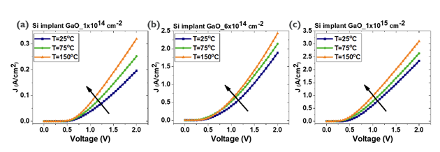
Figure 9. Temperature-dependent I-V characteristics of β-Ga2O3 SBD with Si implantation doses of (b) 1x10^14 cm^-2 (c) 6x10^14 cm^-2 (d) 1x10^15 cm^-2
Conclusion
The EG of β-Ga2O3 reaches 4.8 eV, and its BFOM value is 3444 times that of Si, making it very suitable for power devices. Because of this high EG, the resistivity of undoped β-Ga2O3 is very high, making it unsuitable for semiconductor device fabrication. Therefore, moderate doping is required to enhance carrier concentration and reduce resistivity. N-type β-Ga2O3 commonly uses Si, Ge, and Sn as donors to increase electron concentration. Our team has prepared high-quality, high-crystallinity UID β-Ga2O3 using MOCVD and can significantly control the doping concentration of Si through Si Implantation, which is beneficial for power device fabrication. Our team has also successfully fabricated SBD using Si Implantation β-Ga2O3 and explored the material properties of Si Implantation β-Ga2O3 and the device characteristics of SBD using various measurement techniques. Some of the content and data of this paper have been published in "Electrical performance study of Schottky barrier diodes using ion implanted β-Ga2O3 epilayers grown on sapphire substrates", Materials Today Advanced, 17, 100346, 2023.
Reference:
[1] Xue, H., He, Q., Jian, G., Long, S., Pang, T., & Liu, M. (2018). An overview of the ultrawide bandgap Ga2O3 semiconductor-based Schottky barrier diode for power electronics application. Nanoscale research letters, 13(1), 1-13.
[2] Kotecha, R. M., Zakutayev, A., Metzger, W. K., Paret, P., Moreno, G., Kekelia, B., ... & Graham, S. (2019, October). Electrothermal Modeling and Analysis of Gallium Oxide Power Switching Devices. In International Electronic Packaging Technical Conference and Exhibition (Vol. 59322, p. V001T06A017). American Society of Mechanical Engineers.
[3] Kalarickal, N. K., Xia, Z., McGlone, J., Krishnamoorthy, S., Moore, W., Brenner, M., ... & Rajan, S. (2019). Mechanism of Si doping in plasma assisted MBE growth of β-Ga2O3. Applied Physics Letters, 115(15), 152106.
[4] Ahmadi, E., Koksaldi, O. S., Kaun, S. W., Oshima, Y., Short, D. B., Mishra, U. K., & Speck, J. S. (2017). Ge doping of β-Ga2O3 films grown by plasma-assisted molecular beam epitaxy. Applied Physics Express, 10(4), 041102.
[5] Mauze, A., Zhang, Y., Itoh, T., Ahmadi, E., & Speck, J. S. (2020). Sn doping of (010) β-Ga2O3 films grown by plasma-assisted molecular beam epitaxy. Applied Physics Letters, 117(22), 222102.
[6] Feng, Z., Anhar Uddin Bhuiyan, A. F. M., Karim, M. R., & Zhao, H. (2019). MOCVD homoepitaxy of Si-doped (010) β-Ga2O3 thin films with superior transport properties. Applied Physics Letters, 114(25), 250601.
[7] He, Q., Mu, W., Dong, H., Long, S., Jia, Z., Lv, H., ... & Liu, M. (2017). Schottky barrier diode based on β-Ga2O3 (100) single crystal substrate and its temperature-dependent electrical characteristics. Applied Physics Letters, 110(9), 093503.
[8] Apoorva Sood, Dong-Sing Wuu, Fu-Gow Tarntair, Ngo Thien Sao, Tian-Li Wu, Niall Tumilty, Hao-Chung Kuo, Singh Jitendra Pratap, Ray-Hua Horng, (2023) "Electrical performance study of Schottky barrier diodes using ion implanted b-Ga2O3 epilayers grown on sapphire substrates", Materials Today Advanced, 17, 100346.


