
Development of Scanning Electron Microscopy Analysis Technology - Taking the Analysis of Epitaxial Defects in Wide Bandgap Semiconductors as an Example
The development of scanning electron microscopy analysis techniques
Taking the analysis of epitaxial defects in wide bandgap semiconductors as an example
Professor Zhang Liuwen
Shih Cheng-Hung, Liu Shih-Hui
National Sun Yat-sen University, Department of Materials and Optoelectronic Science
(This article is written by Professor Zhang Liuwen's research team; edited by MA-tek)
-
1. Introduction
The development of scanning electron microscopy (hereinafter referred to as SEM) lagged behind that of transmission electron microscopy (hereinafter referred to as TEM), originating from Knoll's research on television picture tubes. Subsequently, under the continuous research led by teams such as von Ardenne, Zworykin, and Oatlay, the commercialization of SEM was promoted by Cambridge Instrument Company in the early 1960s. After 1965, commercial products of SEM began to appear in Europe and Asia. Since then, SEM has rapidly become an important tool for materials analysis, providing information on material surface morphology and composition distribution. As SEM became increasingly popular, scholars began to explore the possibility of using SEM to capture crystallographic information of materials, further expanding the depth and breadth of SEM applications in materials analysis. Starting in the early 1970s, several important techniques were published, such as electron channeling pattern (ECP), Kossel diffraction pattern (KDP), and electron backscatter diffraction (EBSD), which can acquire electron or X-ray diffraction patterns in SEM. However, before 1990, these techniques were limited by insufficient spatial resolution and analysis speed, making it difficult to promote their application in the study of mainstream metals and ceramics at the time. In the study of semiconductor materials, the key issues at that time were innovations in device miniaturization and metallization processes, thus these techniques also lacked the space to be utilized.
Wide bandgap semiconductors refer to semiconductors with an energy gap (Eg) value above 2.3 eV, whose epitaxial growth technology has received significant attention in the development of blue light-emitting diodes and laser diodes. In particular, the epitaxial growth of wide bandgap semiconductors faces a major challenge due to the lack of homogenous epitaxial substrates and heteroepitaxial substrates with low lattice mismatch, resulting in high-density defects during epitaxy. For a long time, the analysis of epitaxial defects in wide bandgap semiconductors has primarily relied on high-resolution X-ray diffraction and transmission electron microscopy techniques. However, in the past two decades, scanning electron microscopy-based diffraction and imaging techniques have developed rapidly, achieving significant improvements in resolution and analysis speed, opening up opportunities for applications in semiconductor defect analysis. Compared to the statistical distribution information provided by high-resolution X-ray diffraction, scanning electron microscopy analysis can offer precise spatial distribution information; in contrast to the high dependence of transmission electron microscopy on sample preparation techniques, scanning electron microscopy can provide rapid and large-area analysis results in a non-destructive manner. Therefore, the main purpose of this paper is to introduce two scanning electron microscopy-based analytical techniques for the application opportunities in the analysis of epitaxial defects in wide bandgap semiconductors.
This article mainly focuses on several wide bandgap semiconductors with a hexagonal structure, such as Gallium Nitride (GaN, Eg=3.4 eV), Aluminum Nitride (AlN, Eg=6.2 eV), Zinc Oxide (ZnO, Eg=3.3 eV), and Silicon Carbide (4H-SiC/6H-SiC, Eg=2.8-3.2 eV). These wide bandgap semiconductors, especially GaN, AlN, and ZnO, have been widely used in surface acoustic wave devices, ultraviolet and blue light detectors, light-emitting diodes, and laser diodes. In recent years, due to the advantages of wide bandgap semiconductors having large bandgap values, high breakdown voltages, as well as high electron mobility and thermal conductivity, they have become popular candidate materials for applications in high power (voltage) and high frequency devices. In the application of diodes and transistors, wide bandgap semiconductors exist in an epitaxial form to eliminate the significant impact of grain boundaries on carrier conduction. However, the crystalline defects formed during epitaxial growth still scatter electrons or become recombination centers for electrons and holes, leading to a deterioration in carrier mobility or a decrease in quantum efficiency, which affects the performance of the devices. In light of this, the analysis of the types, distribution, and density of defects in the epitaxy of wide bandgap semiconductors is extremely important. In the past, both academia and industry have invested considerable research efforts in the analysis of epitaxial defects and have established a series of analytical methods. This article first provides a brief introduction to the common epitaxial defects in wide bandgap semiconductors and the commonly used analytical methods, and then introduces two analytical techniques developed using scanning electron microscopy as a platform: Electron Channeling Pattern (ECP) and Electron Channeling Contrast Imaging (ECCI), as well as the development of Electron Backscatter Diffraction (EBSD), along with the results achieved by these two techniques in the analysis of defects in wide bandgap semiconductors. Finally, it will look forward to the potential application opportunities of these two techniques in the analysis of defects in wide bandgap semiconductors.
2. Crystal defects and defect analysis of wide bandgap semiconductor epitaxy
2.1. Crystalline Defects in Wide Bandgap Semiconductor Epitaxy
The hexagonal wurtzite structure of wide bandgap semiconductors belongs to the hexagonal crystal system with a lattice constant where the a-axis length ranges between 3.07-3.25 Å. Due to the difficulty in finding suitable epitaxial substrates, these wide bandgap semiconductors are mostly grown on silicon, sapphire, or silicon carbide substrates, resulting in a large lattice mismatch rate between the epitaxy and the substrate, which inevitably leads to a high density of epitaxial defects. Common defects include misfit dislocation, threading dislocation, stacking fault, inversion domain boundary (IDB), mosaic structure, and polytypes, etc. The following will briefly introduce these defects.
- Mismatched dislocations: Mismatched dislocations are dislocation arrays or dislocation networks that arise at the interface between the epitaxy and the substrate due to lattice mismatch between the two, serving to release the elastic strain energy accumulated during the mismatched growth (pseudomorphic growth) process. For polar {0001} epitaxy, the dominant form of mismatched dislocations is in the form of edge dislocations, which release stress in the direction parallel to the substrate surface. However, edge dislocations may also form on the planar steps of a vicinal substrate to release stress in the direction parallel to the growth.
- Penetrating dislocations: Refers to dislocations that extend in the growth direction or at a specific angle to the growth direction in epitaxy. Penetrating dislocations can originate from dislocations that penetrate from the substrate to the surface and continue to grow in the epitaxy. In addition, mismatched dislocations generated during the stress release process may also bend and extend in the growth direction to form penetrating dislocations. Penetrating dislocations include edge dislocations (or type a), screw dislocations (or type c), and mixed dislocations (or type a+c). Furthermore, in the epitaxy of nitrides or silicon carbide, giant screw dislocations with (n>1) can also form, also known as nano- or micropipes.
- Stacking faults: In the epitaxy of wurtzite structure, stacking faults mainly occur on the {0001} plane and can be divided into Shockley-type stacking faults generated by slip, and Frank-type stacking faults caused by the insertion or removal of partial atomic planes. The frequency of stacking faults in non-polar epitaxy is higher than that in polar epitaxy. The stacking faults generated on the {0001} plane in nitride epitaxy can be further classified into four types: , , . In silicon carbide, there are more types of stacking faults [9, 11].
- Inversion domain boundary: The atomic-scale step structure present on the substrate causes the epitaxy on both sides of the step to grow in opposite polarities, forming two domains with opposite polarities, known as inversion domain boundaries. In addition to the opposite polarities, there may also be an additional lattice displacement between the two inversion domain boundaries.
- Ingrained structure: Originating from the island growth in the early stages of epitaxial growth, it is a sub-grain structure formed by the gradual merging of independently nucleated crystalline nuclei. The size of the ingrained structure ranges from tens to hundreds of nanometers, and there are two types of domains based on the orientation differences between the crystalline regions: tilt and twist. In the former, the common rotation axis between the two domains is parallel to the epitaxial surface, while in the latter, the rotation axis is perpendicular to the epitaxial surface.
- Polytype inclusions: During the epitaxial growth of nitrides, inclusions of sphalerite structure may accompany, and during the epitaxial growth of 4H or 6H-SiC, various polytype inclusions may also occur.
2.2. Defect Analysis of Epitaxial Wide Bandgap Semiconductors
For the defects in the epitaxy of wide bandgap semiconductors, the main tools for analysis are optical microscopy, high-resolution X-ray diffraction, transmission electron microscopy, and atomic force microscopy [14-17]. Among them, optical microscopy and atomic force microscopy can be combined with wet etching techniques to observe the morphology and distribution of defects. High-resolution X-ray diffraction analysis can determine the elastic strain and composition in the epitaxy through the identification of lattice constants, and by analyzing the broadening of reciprocal lattice diffraction spots in different crystallographic directions, information about the morphology and average density of epitaxial defects can be obtained. Transmission electron microscopy analysis can utilize convergent beam diffraction to analyze the polarity of the epitaxy, use selected area diffraction and two beam imaging to analyze the morphology and spatial distribution of defects, analyze interface structural characteristics using high-resolution images, and analyze the distribution of specific elements in the epitaxy using high angle annular dark field (HAADF) imaging techniques.
3. Epitaxial Defect Analysis Techniques Based on Scanning Electron Microscopy
Scanning electron microscopy is more convenient to use and has fewer requirements for sample preparation, making it far more popular in general materials analysis applications compared to transmission electron microscopy. However, its application in analyzing epitaxial defects in wide bandgap semiconductors is currently very limited. It is worth noting that, in addition to the significant improvements in the resolution and imaging methods of scanning electron microscopy in recent years, several scanning electron microscopy-based analytical techniques have also advanced rapidly. Coupled with the advantages of non-destructive analysis offered by scanning electron microscopy and the ability to present the spatial distribution characteristics of defects, it is possible that in the near future, scanning electron microscopy could play a more important role in the defect analysis of epitaxial growth in wide bandgap semiconductors. The following discussion will focus on (1) techniques based on electron tunneling effects and (2) techniques based on electron backscatter diffraction.
3.1. Techniques Based on Electron Tunneling Effect
The report on the electron tunneling effect began with two papers published in 1967 in Philosophical Magazine. When the incident direction of the electron beam is nearly parallel to a certain crystallographic plane in the crystal, the backscatter coefficient of the electrons reaches its maximum when the angle (θ) between the electron beam and the crystallographic plane is less than θB (or θ is between +/−θB). When θ is approximately equal to θB, the backscatter coefficient drops sharply to its minimum value, and as θ continues to increase, the backscatter coefficient rises from the trough back to a normal value. The aforementioned θB is the Bragg angle of the crystallographic plane. Therefore, when the focusing lens and scanning coils of the scanning electron microscope are controlled so that the electron beam is incident at an angle of 0-α (for example, α=5°) in a circular direction at the same position of the specimen, due to the aforementioned tunneling effect, two band-like contrasts will form along the direction of this crystallographic plane, with both width and direction identical to that of the Kikuchi band, thus also referred to as the pseudo-Kikuchi band. Using this method, pseudo-Kikuchi patterns of the crystal within the range of +/-5-15° can be obtained, as shown in Figure 1(c), also known as the selected area electron tunneling pattern (SA-ECP). Through the analysis of SA-ECP, the crystallographic orientation at specific locations of the crystal can be obtained. The resolution of SA-ECP for crystallographic orientation can reach 0.5°, but its spatial resolution deteriorates due to the aberration of the objective lenses, only ranging between 1-10µm. In addition, ECP relies on backscattered electron imaging, so the penetration depth of the backscattered electrons contributing to ECP within the specimen is only about 50-150 nm, making it susceptible to interference from the surface state of the specimen. Besides the aforementioned methods, ECP can also be obtained at very low magnifications by utilizing the characteristic of electrons incident at different angles while scanning the surface of the specimen, but this method is only applicable to single crystal specimens.
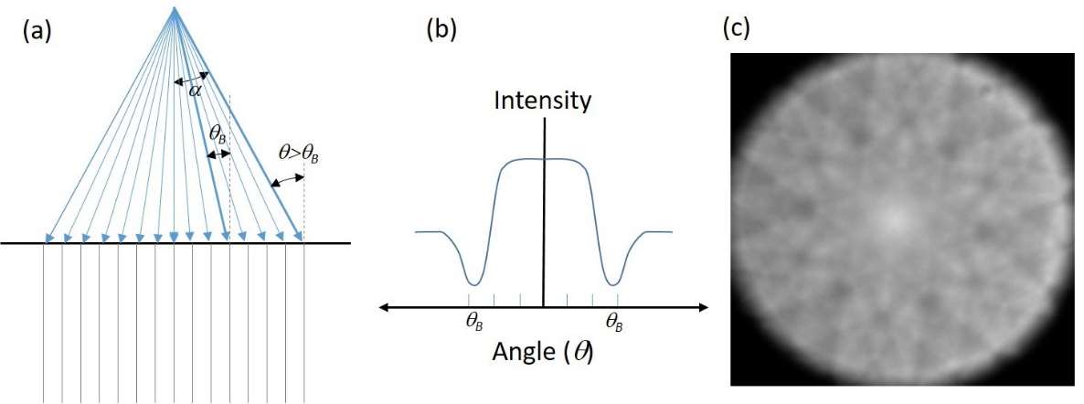
Figure 1. Schematic diagram of the electron tunneling effect: (a) The relationship between the lattice plane and the incident electrons, (b) The relationship between the angle between the incident electrons and the lattice plane and the electron reflection coefficient (or reflected electron intensity), and (c) The simulated Kikuchi pattern formed by GaN epitaxy at an acceleration voltage of 10kV.
In the article by Booker et al. [19] explaining the principle of ECP, it was also predicted that the image contrast generated by the tunneling effect could be used to observe defects in crystals. The principle can be illustrated in Figure 2(a-b). Assuming there is an edge dislocation parallel to the surface, located 10 nm below the surface, when the electron beam is incident at an angle θB (relative to the normal lattice), the angle between the distorted lattice on the right side of the dislocation and the electron beam will be less than θB, resulting in an increased number of backscattered electrons. Conversely, the angle between the distorted lattice on the left side of the dislocation and the electron beam will be slightly greater than θB, leading to a decrease in the number of backscattered electrons to a minimum, creating a black and white contrast in the dislocation image. The above analysis assumes that the electron beam is perfectly parallel and has a very small diameter. In practical operation, it is necessary to ensure that the electron beam diameter is less than 10 nm and to minimize the convergent angle (approximately below 10 mrad) to obtain a clear backscattered electron image of the dislocation under appropriate conditions, which is known as the electron channeling contrast image (ECCI). In recent years, due to the rapid development of field emission scanning electron microscopy, the imaging of ECP and ECCI has become increasingly easier. Figure 2(c) shows an ECCI image of gallium nitride epitaxy taken with a Zeiss Gemini 450 SEM using a 10 kV, 4 nA electron beam, where both vertical and parallel dislocations to the sample surface are present. The former creates a black and white contrast resembling a double-lobed structure, as indicated by the red circle in Figure 2(c), while the latter appears as black lines, as shown by the red arrow in Figure 2(c). However, at the point where it penetrates the surface, it exhibits the same point-like black and white contrast as the former. For the influence of scanning electron microscope operating conditions on ECP and ECCI imaging, readers can refer to reference [20]. Additionally, ECP and ECCI imaging can also be performed under conditions where the sample is highly tilted. When the sample is tilted at 70° (which is the typical condition for performing EBSD analysis), the number of forward scattered electrons generated in the direction where the angle relative to the electron beam incident direction is 30-40° (i.e., with an angle of 10-20° to the sample surface) is several times that of vertical incidence, and the energy loss of the electrons is also relatively small, making it easier to obtain high-contrast ECCI images. Figure 3 is a schematic diagram of the imaging modes of these two types of ECP and ECCI [21].
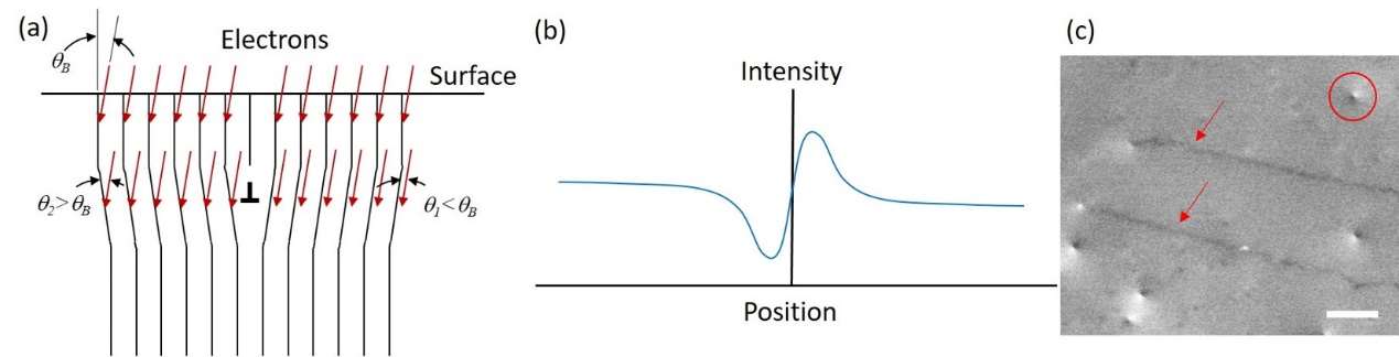
Figure 2. Schematic diagram of the transistor structure from IMEC [2]. When the sub-surface dislocation is incident at an angle close to the Bragg angle, (a) the relationship between the electron beam direction and the lattice planes, and (b) the intensity distribution of backscattered electrons near the dislocation core. (c) ECCI image of GaN epitaxial film.
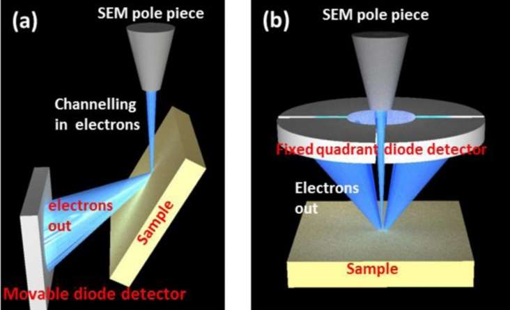
Figure 3. Schematic diagram of the positions of the electron beam, specimen, and backscattered electron detector for the two methods of obtaining ECP patterns and ECCI images: (a) the angle between the specimen normal direction and the electron beam is 70 degrees, and (b) the specimen normal direction is parallel to the electron beam [21].
For the polarity surface epitaxy of zinc blende wide bandgap semiconductors, the lattice distortion around c-type screw dislocations is greater than that of a-type edge dislocations. Therefore, the size of the tunneling effect produced by the former in ECCI images will also be larger than that of the latter. Figure 4 shows the ECCI image of gallium nitride epitaxy, where two types of penetrating dislocations can be seen, as indicated by the solid and dashed circles. The one with strong contrast is the screw dislocation, while the one with weak contrast is the edge dislocation, which is more numerous [22]. Figure 5 is the ECCI image of 4H silicon carbide epitaxy, showing that the screw penetrating dislocation presents a symmetric dark double-lobed contrast when it just meets the two-beam condition. When slightly deviating from the two-beam condition (i.e., s>0 or s<0), it presents a black and white double-lobed contrast, with the vector from black to white being perpendicular to the corresponding reciprocal lattice vector (ghkil) of the crystal plane being imaged. For a-type edge dislocations, the vector from black to white is perpendicular to its Burgers vector, while for a+c type mixed dislocations, the direction of the vector from black to white is determined by the components of the edge dislocation and screw dislocation. Through the extinction condition relationship, edge dislocations and screw (or mixed) dislocations can be distinguished, but screw dislocations and mixed dislocations cannot be differentiated [23]. Naresh-Kumar et al. [24] proposed another method to identify dislocation types, using ECP spectra to find two sets of Kikuchi bands belonging to the same plane family. For example, in Figure 6(a), there are two sets of Kikuchi bands belonging to the planes, with an angle of 120 degrees between them. Therefore, ECP and ECCI images are captured under two different two-beam conditions, as shown in Figures 6(b-e). The black and white contrast vector of the penetrating dislocation in ECCI can be used to determine the type of dislocation. As shown in the red circles in Figures 6(c) and (e) (enlarged in Figures 6(f) and (i)), the black and white contrast vectors are both perpendicular to the g vector, indicating they are screw dislocations. The black and white contrast in the green squares (enlarged in Figures 6(g) and (j)) rotates 180 degrees only due to the change in two-beam conditions, indicating they are edge dislocations. The blue octagons (enlarged in Figures 6(h) and (k)) represent mixed dislocations, whose black and white vector direction changes differently from the aforementioned two. In addition, the mismatch dislocations between the epitaxy and substrate can also be observed when the epitaxial thickness is less than about 100 nm. Figure 6 shows the ECCI image of mismatched dislocations generated at the interface between silicon and gallium phosphide, grown to a thickness of 50 nm on a silicon substrate [25].
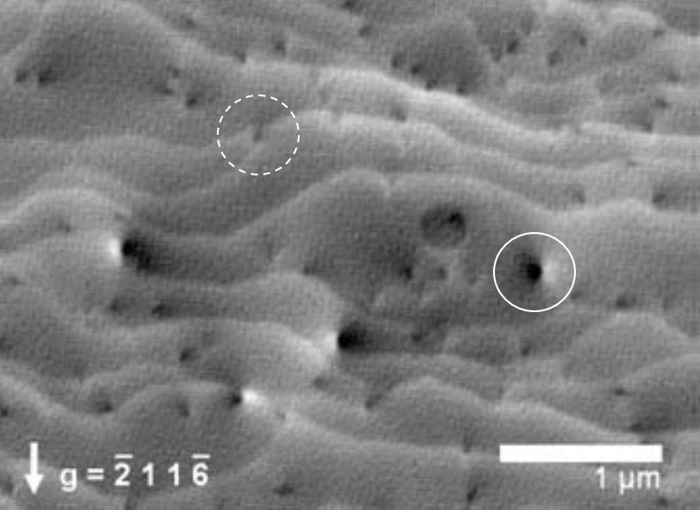
Figure 4. ECCI images of the GaN epitaxial sample formed under dual beam conditions in the mode shown in Figure 3(a). The penetrating dislocations in the figure can be classified into two types: those with strong contrast (as indicated by the solid circle) and those with weak contrast (as indicated by the dashed circle) [22].
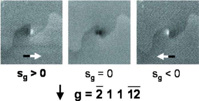
Figure 5. ECCI images of 4H-SiC epitaxial samples formed under three dual beam conditions (s>0, s=0, s<0) [23].
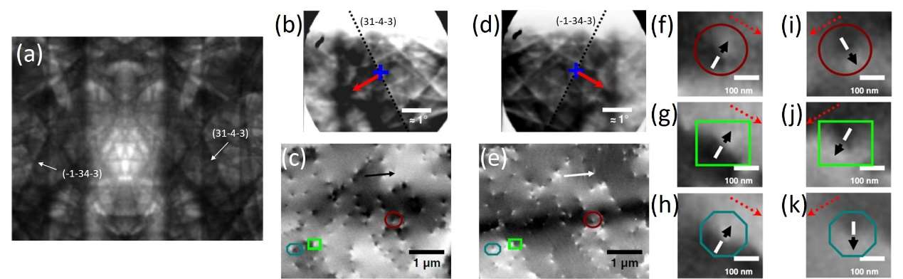
Figure 6. (a) Simulated Kikuchi pattern of GaN epitaxy, (b) ECP and (c) ECCI obtained at g=31-4-3, and (d) ECP and (e) ECCI obtained at g=-1-34-3, as well as the magnified ECCI image from (c): (f) red circular, (g) green square, and (h) blue octagonal regions, and the magnified ECCI image from (e): (i) red circular, (j) green square, and (k) blue octagonal regions (reproduced from literature [24])
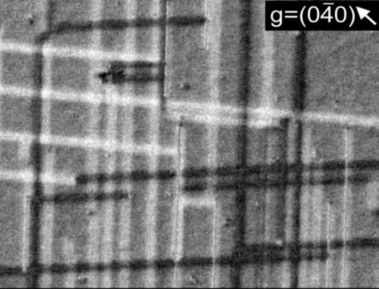
Figure 7. ECCI image of mismatched dislocations generated at the interface of 50nm thick gallium phosphide grown on silicon substrate [25]
In addition to imaging various defects, atomic-scale step structures formed on the surface during epitaxial growth can also be observed in ECCI images, which are caused by localized atomic structure distortions at the step edges. In the ECCI image of GaN epitaxy shown in Figure 4, clear atomic-scale step structures can be seen.
3.2. Electron Backscatter Diffraction Technique
Compared to the development of ECP technology, the electron backscatter diffraction (EBSD) technique executed under the scanning electron microscope was published several years later. The EBSD system uses a specimen with an electron beam incident at an angle of 70 degrees, utilizing the scattered incident electrons, which produce diffraction during the process of leaving the specimen, forming a Kikuchi pattern on the screen in front of the specimen. By using relevant geometric parameters (including the electron beam irradiation position, specimen coordinates, and screen coordinates, etc.), the crystallographic orientation can be identified based on the Kikuchi pattern. In Figure 3(a), the movable diode detector in front of the specimen is replaced with an EBSD detector, which is the most common EBSD analysis configuration today. Early EBSD systems used cameras to record the Kikuchi pattern on the fluorescent screen and then calculated the crystallographic orientation in a semi-automatic manner. As a result, identifying a Kikuchi pattern took several tens of seconds. In the early 1990s, Krieger Lassen and others developed a technique for automatic identification of Kikuchi patterns through the Hough transform, significantly speeding up the analysis. By 1995, with the introduction of CCD cameras to record Kikuchi patterns, the analysis speed of EBSD could reach around 1-10 Hz. Subsequently, with the continuous optimization of scanning electron microscopes, CCD cameras, and analysis software, along with the adoption of CMOS cameras, the analysis speed gradually increased to 1000-5000 Hz (see Figure 8). Since the Kikuchi pattern of EBSD is captured in a momentarily stationary state of the electron beam, the clarity of the Kikuchi pattern mainly depends on the atomic number of the material, the electron acceleration voltage, and the surface state of the specimen. When the analysis speed increased from 10 Hz to 1000 Hz, the time required to perform a 500 x 500 pixel orientation imaging map could be significantly reduced from 7 hours to 4 minutes, comparable to the time required for a composition distribution map using silicon drift energy dispersive spectrometry (SD-EDS). Thus, the analysis of the scanning electron microscope has entered a new stage of integrated imaging, crystallographic orientation, and composition analysis.
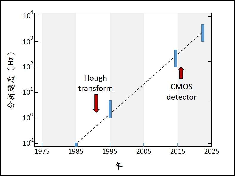
Figure 8. Evolution of EBSD analysis speed.
The angular range covered by the Kikuchi pattern of EBSD is much greater than that of ECP, so multiple zone axes can appear in a single Kikuchi pattern, allowing for accurate determination of the crystallographic orientation. However, in the surface analysis of EBSD, variations in the analysis position and the height of the analyzed sample can cause errors in the calculation of the crystallographic orientation. Therefore, generally speaking, the angular resolution of EBSD for crystallographic orientation is about 0.1° to 1°, while its spatial resolution is closely related to the atomic number of the material and the electron acceleration voltage. For GaN, under an acceleration voltage of 20 kV, the lateral spatial resolution is about 50 nm.
Through EBSD analysis of crystal structure and crystallographic orientation, it is easy to identify the types, sizes, and distributions of inclusions in the epitaxial layer. Figures 9(a-b) show the EBSD analysis results of the inclusions defects that appeared in the homogeneously grown epitaxial layer on a 4H-SiC substrate cut at a 4° angle, indicating that the inclusions are inclined growing 3C-SiC layers. Figures 9(c-d) display the secondary electron images and EBSD phase distribution maps of the magnesium-doped zinc oxide epitaxy with rocksalt (RS) structure grown on a (100) MgO substrate, clearly showing the distribution characteristics of the wurtzite (WZ) structure islands. In addition to identifying crystal structures, the polarity of non-centrosymmetric wurtzite and zinc blende structured wide bandgap semiconductors can also be determined through crystallographic orientation analysis. Figures 10(a-b) take GaP with a zinc blende structure as an example, showing the two opposite direction Kikuchi patterns obtained through simulation, indicating that the black and white contrast in the two {111} Kikuchi bands is symmetrically distributed along the center of the Kikuchi bands. Therefore, as shown in Figure 10(c), after subtracting the two, the differences are clearly presented in the two {111} Kikuchi bands. Figure 10(d) shows the results of determining the polarity of GaN nanocolumns using the above method. This technique can also analyze whether there are anti-polar domains in the epitaxy and identify the boundaries of anti-polar domains.
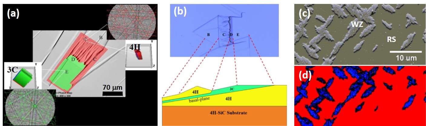
Figure 9. (a) EBSD analysis results of the epitaxial layer homogeneously grown on a 4H-SiC substrate with a 4° tilt, (b) optical photo of the defect area and schematic diagram of the defects, (c-d) island-like wurtzite structure appearing in magnesium-doped zinc oxide epitaxy grown on MgO substrate (secondary electron image of WZ epitaxy (c) and EBSD phase distribution map (d) (reproduced from references 28 and 29).
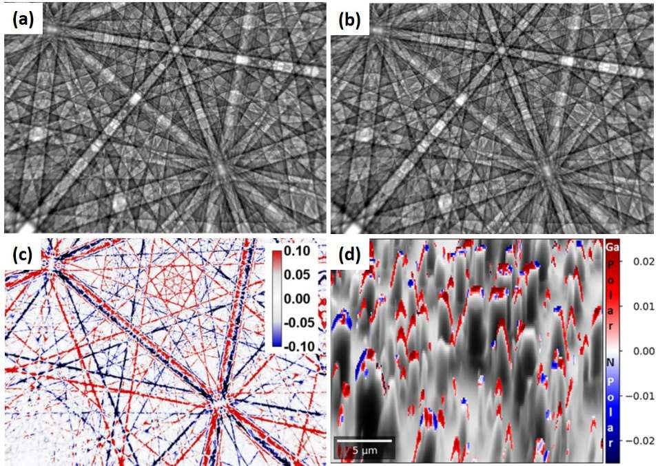
Figure 10. The Kikuchi patterns of GaP obtained from simulations in the directions of (a) P2=43.1° and (b) P2=133.1°, (c) the intensity distribution map after subtracting the two, and (d) the polarity distribution of GaN nanocolumns obtained using EBSD analysis. (Reproduced from references 30 and 31)
The defects that are more commonly found in epitaxy include dislocations, stacking faults, and precipitate structures. The lattice distortions caused by the stress field around these defects can lead to rotations of the crystallographic orientation and changes in the angle between the crystal axes. According to estimates by Booker et al. [19], the amount of lattice rotation at a distance of 30 nm from a single dislocation core is approximately 0.05° (10-3 rad), which is below the angular resolution range of the aforementioned EBSD. Therefore, in recent years, scholars have been dedicated to developing high-resolution EBSD analysis techniques (also known as HR-EBSD). Among them, the technique developed by Professor Wilkinson from the University of Oxford is the most mature. This technique involves selecting a Kikuchi pattern from an m×n pixel area scan as a reference Kikuchi pattern and then comparing Kikuchi images from four or more regional areas in other Kikuchi patterns with the regional Kikuchi pattern at the same position as the reference Kikuchi pattern. This allows for the calculation of the relative crystal rotation and relative displacement between the two, facilitating detailed calibration of the crystallographic orientation and strain distribution calculations. This method can enhance the angular resolution of EBSD to about 0.01°-0.05° and resolve strains greater than 1×10⁻⁴ [32]. In other words, it is already sufficient to analyze the strain distribution around defects such as dislocations, stacking faults, and precipitate structures.
Recently, there have been some applications of HR-EBSD technology in the defect analysis of epitaxial wide bandgap semiconductors. For example, Ernould et al. [33] used HR-EBSD analysis, combined with finite element method applications, to analyze giant screw dislocations (Giant screw dislocation or nanopiple) in GaN epitaxy, determining that the Burgers vector of the observed giant screw dislocation is three times the c-axis length. Ruggles et al. [34] used HR-EBSD technology to analyze a type of star-shaped defect in GaN epitaxy, identifying that this defect, which reaches hundreds of micrometers in size, is composed of a large number of edge dislocations on a-type pyramidal planes, stacking into six low-angle grain boundaries without damaging the epitaxy. Wilkinson's team [35] simultaneously employed ECCI imaging analysis technology and HR-EBSD technology to analyze the penetrating dislocation defects in indium aluminum nitride (InAlN) epitaxy grown on silicon carbide and sapphire substrates. By taking ECCI images under two different imaging conditions, the changes in the black-and-white contrast vector at the dislocation center were used to identify edge dislocations and screw dislocations (including mixed dislocations), thus obtaining their densities. Then, using the strain and rotation values obtained from HR-EBSD technology, the densities of edge dislocations (including mixed dislocations) and screw dislocations were calculated through the gradient functions based on Nye-Kroner's theory [36]. The results are shown in Table 1, consistent with the results from transmission electron microscopy, indicating that edge dislocations are predominant in both types of epitaxy, and the dislocation density analyzed by transmission electron microscopy is slightly higher than that obtained from ECCI and HR-EBSD analysis.
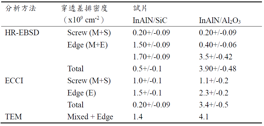
Table 1: Results of the dislocation density obtained from the analysis of aluminum indium nitride (InAlN) epitaxy grown on silicon carbide and sapphire substrates using ECCI and HREBSD techniques [35].
Conclusion
From the introduction of several analysis techniques based on scanning electron microscopy mentioned above, it can be seen that for the analysis of epitaxial wide bandgap semiconductors, it is most suitable to use a large-angle inclined electron beam. By utilizing the secondary electrons generated in large quantities, ECCI images can be formed, allowing simultaneous EBSD, EDS, SEI, CL (cathodoluminescence), and even EBIC (electron beam induced current) analysis. Under this framework, the topological changes in the surface of the specimen are also easily highlighted. However, the current scanning electron microscope has serious limitations on specimen size and movement when the specimen is placed at a high angle of inclination, and it is not easily compatible with CL and EBIC systems.
To overcome this issue, if the current scanning electron microscope can be modified to the configuration shown in Figure 11, tilting the axis of the electron gun and electromagnetic lens system from the original vertical downward to an angle of 50° to 70°, and incident on the sample at an angle of 20° to 40°, using an Eulerian cradle that can provide three-axis movement and tilting to support the sample, the EBSD detector, CL mirror, BSD detector, SE detector, EDS detector, and EBIC probe can all be configured above the sample. Therefore, the sample stage can support 4-8 inch wafers, providing a tilt of approximately +30°/-5° along the x-axis, as well as a 360° rotation along the sample normal direction, allowing analysis of any position on the wafer. For ECP and ECCI, it can be completed in a few minutes, while the high-resolution Kikuchi pattern required for HR-EBSD takes about 10-60 minutes. If only analyzing the total dislocation density in the epitaxy, sufficient sample numbers for analysis can be obtained within 30-60 minutes. If a more precise estimate of dislocation types and quantities is needed, the analysis time is about 1-4 hours. Additionally, completed components can also be analyzed using EBIC technology. The aforementioned analysis times are similar to those required for high-resolution X-ray diffraction and transmission electron microscopy analysis, thus providing strong support for quality control and research and development activities.
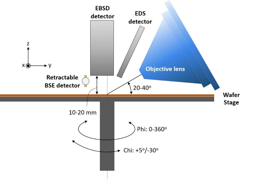
Figure 11. Possible architecture of scanning electron microscopy applied to defect analysis of large-size wafers.
Reference:
[1] McMuullan, Scanning, 17 (1995) 175.
[2] D. G. Coates, Phil. Mag, 16 (1967) 1179.
[3] E. T. Peter and R. E. Ogilvie, Trans. Met. Soc. AIME, 233 (1965) 89.
[4] J. A. Venables and C. J. Harland, Phil. Mag., 27 (1973) 1193.
[5] Man Hoi Wong, Oliver Bierwagen, Robert J. Kaplar, Hitoshi Umezawa, J. Mater.Res., 36 (2021) 4601.
[6] Haiwei Jin, Li Qin, Lan Zhang, Xinlin Zeng, Rui Yang, MATEC Web Conf., 40(2016) 01006.
[7] Krishna Shenai, Michael Dudley, Robert F. Davis, ECS J. Solid State Sci. Technol.,2 (2013) N3055.
[8] X. H. Wu, L. M. Brown, D. Kapolnek, S. Keller, B. Keller, S. P. DenBaars, J. S.Speck, J. Appl. Phys., 80 (1996) 3228.
[9] V. Lebedev, K. Tonisch, F. Niebelschütz, V. Cimalla, D. Cengher, I. Cimalla, Ch.Mauder; S. Hauguth, O. Ambacher, F. M. Morales, J. G. Lozano, and D. González,J. Appl. Phys., 101 (2007) 054906.
[10] J. A. Powell and D. J. Larkin, Phys. Stat. Sol. B, 202 (1997) 529.
[11] G. Feng, J. Suda, T. Kimoto, Appl. Phys. Lett., 94 (2009) 091910.
[12] L. T. Romano, J. E. Northrup, and M. A. O’Keefe, Appl. Phys. Lett., 69 (1996)2394.
[13] V. Lebedev, K. Tonisch, F. Niebelschütz, V. Cimalla, D. Cengher, I. Cimalla, Ch.Mauder; S. Hauguth, O. Ambacher, F. M. Morales, J. G. Lozano, and D. González,J. Appl. Phys., 101 (2007) 054906.
[14] M A Moram and M E Vickers, Rep. Prog. Phys., 72 (2009) 036502.
[15] P. Ma, J. Ni, J. Sun, X. Zhang, J. Li, and H. Chen, Appl, Optics, 59 (2020) 1746.
[16] H. Morkoç, Mater. Sci. Eng. R, 33 (2001) 135.
[17] S. Kaiser, H. Preis, W. Gebhardt, O. Ambacher, H. Angerer, M. Stutzmann, A.Bosenauer, and D. Gerthsen, Jpn. J. Appl. Phys., 37 (1998) 84.
[18] C Trager-Cowan, Semicond. Sci. Technol., 35 (2020) 054001.
[19] G. R. Booker, A. M. B. Shaw, M. J. Whelan, and P. B. Hirsch, Philos. Mag., 16(1967) 1185.
[20] A. J. Wilkonson and P. B. Hirsch, Micron, 28 (1997) 279.
[21] G. Naresh-Kumar, D. Thomson, M. Nouf-Allehiani, J. Bruckbauer, P. R.Edwards, B. Hourahine, R. W. Martin, C. Trager-Cowan, Mater. Sci. Semicon.Process., 47 (2016) 44.
[22] Y. N. Picard, M. E. Twigg, J. D. Caldwell, C.R. Eddy Jr., M. A. Mastro, R. T.Holm, Scripta Mater., 61 (2009) 773.
[23] Y. N. Picard, M. E. Twigg J. Appl. Phys. 104 (2008) 124906.
[24] G. Naresh-Kumar, B. Hourahine, P. R. Edwards, A. P. Day, A. Winkelmann, A. J.Wilkinson, P. J. Parbrook, G. England, and C. Trager-Cowan, Phys. Rev. Lett.,108 (2012) 135503.
[25] S. D. Carnevale, J. I. Deitz, J. A. Carlin, Y. N. Picard, M. De Graef, S. A. Ringel, T. J. Grassman, Appl. Phys. Lett., 104 (2014) 232111.
[26] J. A Venables and C. J. Harland, Phil. Mag., 27 (1973) 1193.
[27] N. C. Krieger Lassen, Mater. Sci. Technol., 12 (1996) 837.
[28] J. Hu, R. Jia, Y. Niu, Y. Zang, H. Pu, J. Cryst. Growth, 506 (2019) 14.
[29] C.-Y. J. Lu, Y.-T. Tu, T. Yan, A. Trampert, L. Chang, and K. H. Ploog, J. Chem.Phys., 144 (2016) 214704.
[30] A. Winkelmann, G. Nolze, Appl. Phys. Lett., 106 (2015) 072101.
[31] G. Naresh-Kumar, J. Bruckbauer, A. Winkelmann, X. Yu, B. Hourahine, P. R.Edwards, T. Wang, C. Trager-Cowan, R. W. Martin, Nano Lett., 19 (2019) 3863.
[32] A. J. Wilkinsona, G. Meadenb, D. J. Dingley, Ultramicroscopy, 106 (2006) 307.
[33] C. Ernould, V. Taupin, B. Beausir, J.J. Fundenberger, N. Maloufi, J. Guyon, E.Bouzy, Mater. Charact., 194 (2022) 112351.
[34] T. J. Ruggles, J. I. Deitz, A. A. Allerman, C. Barry Carter, J. R. Michael, Microsc.Microanal., 27 (2021) 257.
[35] A. Vilalta-Clemente, G. Naresh-Kumar, M. Nouf-Allehiani, P. Gamarra, M.A. diForte-Poisson, C. Trager-Cowan, A.J. Wilkinson, Acta Mater., 125 (2017) 125.
[36] E. Kroner, Ergeb. Angew. Math., 5 (1958) 1327.


