
The role of crystal structure in semiconductors and the application of X-ray diffraction analysis.
With the advancement of technology and the development of advanced processes, electronic products are becoming smaller and smaller, and the size of semiconductor components is approaching the physical limits of materials. In order to meet the demands of next-generation electronic products, such as small size, multifunctionality, fast instruction cycles, and low power consumption, while avoiding the physical limits of component size, surpassing Moore's Law has become the current research goal of the semiconductor industry.
In the situation where it is no longer possible to continue reducing the size of semiconductor components through processes, most of the semiconductor industry has begun to move towards technologies that achieve the miniaturization of semiconductor components through three-dimensional stacking processes, such as 3D packaging technology. By stacking each chip layer in the vertical direction, the number of components per unit area can be increased, allowing the manufacturing costs of semiconductor components to continue to decrease. In addition, integrating different functional components together enables the components to have more diverse capabilities.
In addition to changes in process technology, the research and development of novel materials is also a focus for major semiconductor companies at present, such as compound semiconductor materials like Gallium Nitride (GaN), Silicon Carbide (SiC), and Indium Phosphide (InP), because compound semiconductor materials have characteristics such as: direct bandgap, high breakdown voltage, and high electron mobility.
The semiconductor industry, as one of the important industries, is most directly related to the materials themselves in terms of semiconductor component characteristics. The performance of materials depends on their organizational structure, which is closely related to factors such as chemical composition, bonding methods, and arrangement methods. This article mainly introduces the application cases of X-ray diffraction analysis (XRD) in quality control monitoring analysis in semiconductor processes.
Case 1 Understanding of Single Crystal, Polycrystal, and Amorphous
The material structure is composed of atomic arrangements. A single crystal has atoms arranged in a regular pattern within a spatial lattice; a polycrystal consists of multiple different arrangements of single crystals within a spatial lattice; and an amorphous structure lacks any long-range ordered arrangement. The different arrangement conditions have a significant impact on the application of materials. Taking solar cells as an example, solar cells are a type of photovoltaic device that converts energy, where semiconductor materials absorb sunlight to generate electric current for power generation. Among them, silicon solar cells can be divided into three types: monocrystalline silicon, polycrystalline silicon, and amorphous silicon solar cells (as shown in Figure 1). Monocrystalline silicon has the best conversion efficiency and a longer lifespan, but its manufacturing cost is high, making it suitable for use in power plants or traffic lighting signals; polycrystalline silicon, while slightly lower in power generation efficiency than monocrystalline silicon, has a relatively lower cost and simpler manufacturing process, currently being the mainstream in the solar cell market; amorphous silicon has the lowest conversion efficiency, but its advantages include fast production speed and lower price, requiring only micrometer-level coating to be effective. It is currently widely used in thin-film solar panels, suitable for windows, portable charging sources, and in recent years has been applied in RVs, building facades, and portable solar charging panels. Through XRD analysis, the arrangement of the material's crystal structure can be obtained, as shown in Figure 2.
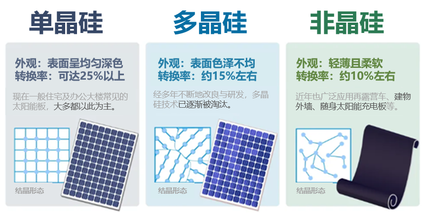
Figure 1. The conversion efficiency and applications of different types of silicon solar cells. (Source - Chengyue Energy Solar Panel Type Differences)
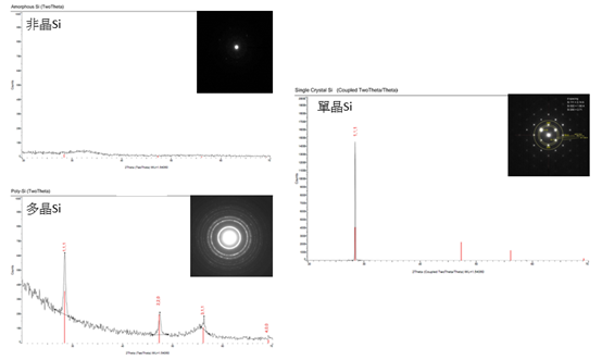
Figure 2. Materials can be distinguished through XRD spectra or selected area diffraction patterns from TEM.
Case 2 The influence of crystal orientation, grain size, and crystallinity on material properties
In addition to the crystal structure, the grain size and crystallinity of the material also affect its mechanical properties (elasticity, plasticity, stiffness, strength, hardness, etc.) and physical properties (electric, magnetic, optical, thermal, etc.).
Grain size essentially reflects the surface area of grain boundaries. The smaller the grains, the larger the surface area of the grain boundaries, which has a greater impact on material performance. In terms of mechanical properties of metals, smaller grains result in higher strength and hardness, as well as better plasticity and toughness. Regarding electrical properties, larger grains indicate fewer grain boundaries, which means less resistance during the electron migration process, leading to higher mobility, implying that larger grains are better for electron transmission. XRD analysis can provide grain sizes in the range of mm to cm and the distribution of crystal orientations (as shown in Figure 3); while Electron Back Scatter Diffraction (EBSD) can perform similar analysis on localized small areas (in the micrometer range) (as shown in Figure 4).
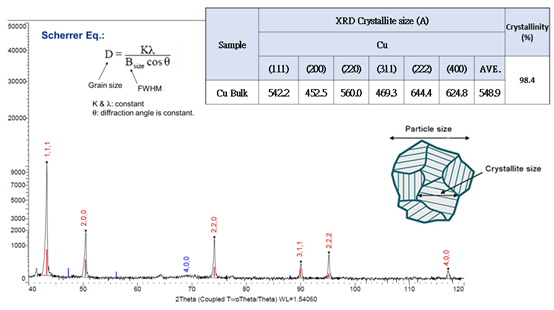
Figure 3. Analysis of the crystal orientation of the copper block material, average grain size for each crystal orientation, overall average grain size, and crystallinity.
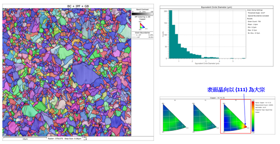
Figure 4. EBSD analysis of the crystal orientation and grain size distribution of the copper block shows that the predominant crystal orientation is {111}.
With the advancement of technology, semiconductor components are becoming smaller, and the thickness of coatings also needs to be reduced, which limits grain growth in the materials. At this point, the crystallographic orientation has an increasing effect on the performance of the components, such as electron mobility. Taking undoped silicon wafers as an example, the conductivity of crystal orientations {111} and {112} is better than that of {100} and {110}; while for copper, the conductivity of the {100} orientation is better than that of {111}. Therefore, during the research and development process of semiconductor components, the crystallographic orientation of the materials also needs to be considered (as shown in Figures 5 and 6).
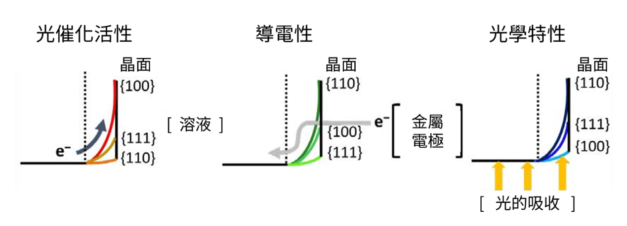
Figure 5. Comparison of the differences in material properties for different silicon crystal orientations. (Source: The Journal of Physical Chemistry C, 122 (24), 13027-13033.)
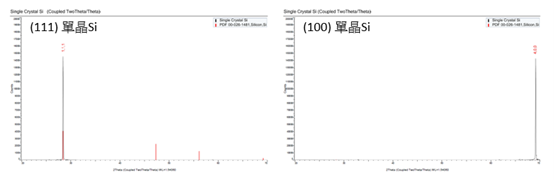
Figure 6. XRD analysis of different components, (left) FRD substrate crystal orientation is (111); (right) IGBT substrate crystal orientation is (100).
When observing the crystal structure of films thicker than several tens of nanometers, low-angle X-ray diffraction (GIXRD) is usually used to extend the path length of X-rays in the material, thereby increasing the diffraction signal of the film. By setting the theoretical density of the material and the incident angle, the penetration depth of the X-ray into the film during low-angle diffraction analysis can be controlled (as shown in Figures 7 and 8).
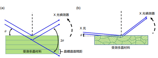
Figure 7. Schematic diagrams of traditional X-ray diffraction (a) θ-2θ scanning mode and (b) low-angle incidence scanning mode. (Source: Instrumentation Column_Application of In-Plane Low-Angle X-ray Diffraction in the Crystal Analysis of Two-Dimensional Materials)
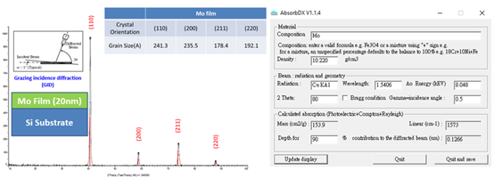
Figure 8. (Left) Analysis of the crystal orientation and grain size of molybdenum thin films using a low angle approach. (Right) At an incident angle of 0.5 degrees, the penetration depth of X-ray into the molybdenum thin film is approximately 126nm.
For coatings with a film thickness of only a few nanometers, or even a few Å for two-dimensional materials, the lattice layers in the vertical direction are too thin, making it insufficient to obtain effective diffraction signals even using GIXRD analysis. However, in-plane low-angle diffraction technology (In-plane GID) provides a good analytical method, overcoming the challenges of ultra-thin films with non-destructive analysis to obtain information on material crystallographic orientation, grain size, and crystal structure. This technology mainly extends the structural method of thin films/materials in the plane, increasing the path of X-rays traveling within the film to obtain effective diffraction signals, and significantly reduces the X-ray penetration depth compared to low-angle diffraction, further decreasing the substrate signal (as shown in Figures 9 and 10).
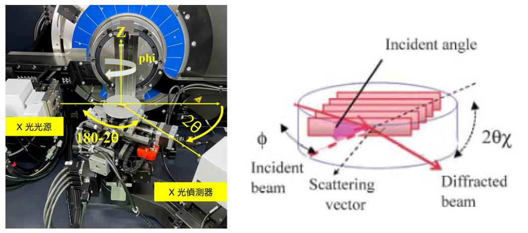
Figure 9. Schematic diagram of the geometric structure in the in-plane low-angle XRD (In-plane GID) scanning mode. (Source: (Left) Scientific Instrument Column_Application of In-plane Low-angle X-ray Diffraction in the Crystal Analysis of Two-dimensional Materials; (Right) Schematic diagram of In-plane GID scanning (Source: The Rigaku Journal, 26(1), 2010.)
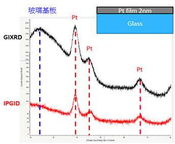
Figure 10. Comparison of low-angle diffraction and in-plane grazing incidence diffraction (In-plane GID) analysis on 2nm Pt deposited on glass, where In-plane GID can effectively reduce background noise.
Case 3: Thin Film Thickness Analysis
In the semiconductor coating process, it is necessary to adjust the process parameters to control the coating rate, so that the coating reaches the specified thickness. Thickness analysis can be performed using the X-ray reflectivity (XRR) technique in XRD without breaking the wafer. Compared to the XRR technique, TEM analysis can obtain region-specific (nm-level) precise thickness values and observe subtle changes on the surface; whereas XRR can measure the film thickness, density, and surface/interface roughness of larger areas (mm-level) (as shown in Figure 11).
__26D208hC1q.png "11 (1)")
Figure 11. (Left) XRR spectra and fitting analysis results before and after etching of SiGe films; (Right) TEM cross-sectional results before and after etching of SiGe films, showing similar trends.
Case 4 Coating/Epitaxial Quality Analysis (Rocking Curve Analysis)
Mobile communication is an essential tool in modern life, where the filtering circuits in communication systems determine communication quality. AlN filters, due to their advantages of high-frequency operation, high temperature stability, and compatibility with CMOS nanoscale, can achieve integration of filtering chips, meeting the demands for compactness and lightweight in mobile communication, thus becoming the main force in the production of filtering chips. In the current 5G communication era, the requirements for filters in mobile communication components are even higher, not only needing to meet high-frequency operation but also having a larger bandwidth and a lower signal loss Q value. In recent years, researchers have found that the stress generated by doping Sc atoms into AlN allows ScxAl1-xN to exhibit better piezoelectric performance than AlN (Source: Science Instrumentation New Knowledge Issue 233: ScxAl1-xN Piezoelectric Resonators Achieve 5G Millimeter Wave Mobile Communication Integration). However, how to detect whether high-quality AlScN films have grown on silicon substrates has become an important issue for communication component manufacturers. For monitoring coating quality, the Rocking Curve method in XRD can be used for inspection. When the crystal structure is orderly arranged, by oscillating the ω axis at a specific diffraction peak, the diffraction intensity will significantly decrease once the ω angle is changed due to non-compliance with Bragg's law; conversely, in a randomly arranged lattice, since there are specific diffraction peak components in all directions, the intensity of that diffraction peak decreases slowly as the ω axis oscillates, as shown in Figure 12.
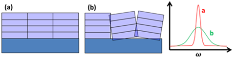
Figure 12. The effect of the lattice stacking arrangement of the coating on the Rocking Curve.
Figure 13 shows that both stacked structures of AlScN exhibit good (002) preferred orientation. However, from the analysis results of the Rocking Curve, it can be clearly observed that the half-width of the left image is narrower, indicating that the stacking structure is more helpful for the arrangement of AlScN on the surface.
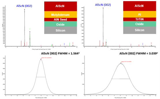
Figure 13. (Top) XRD analysis results of the coating, AlScN shows a good (002) preferred orientation; (Bottom) Analysis results of the Rocking Curve for AlScN (002), the left image has a narrower full width at half maximum, indicating that the stacking structure is more helpful for the arrangement of AlScN on the surface.
Case 5: HRXRD & RSM Observation of Silicon-Germanium Heteroepitaxial Films
In the evolution of Si MOSFET device process miniaturization, how to increase the mobility of electrons and holes in the channel is an important issue for enhancing device performance. Among the methods to improve electron and hole mobility, Strained Engineering (Strained-Si) is one of the most effective methods to enhance the performance of Si nano-devices. Among them, SiGe is one of the most attractive PMOS materials in strained engineering, as SiGe has a higher hole mobility than Si, better Negative Bias Temperature Instability (NBTI) reliability, and a better lattice matching with the Si substrate.
Due to the similar crystal structures and close lattice spacings of Si and SiGe, the diffraction peak positions of both almost overlap when analyzed using conventional diffraction methods. At this point, it is necessary to equip single crystal components to improve the angular resolution of XRD and the collimation of the incident light, so that the analysis results have higher sensitivity to lattice changes. Figure 14 shows the SiGe diffraction peaks obtained through HRXRD analysis. By fitting the relative positions of these diffraction peaks using software, the proportion of each layer of SiGe can be obtained, and the periodic oscillation of the satellite peaks around the diffraction peaks can provide the corresponding thickness of each layer.
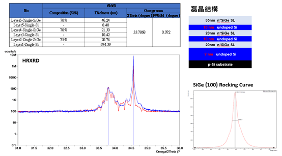
Figure 14. HRXRD analysis results of multilayer SiGe and Si epitaxy. By fitting the relative positions of the diffraction peaks through software, the proportional relationships of each layer of SiGe can be obtained, while the periodic oscillation of the satellite peaks around the diffraction peaks can provide the corresponding thickness of each layer.
In the process of SiGe epitaxial growth, in order to maintain the integrity and continuity of the atomic bonding at the Si and SiGe interface, the lattice spacing of the SiGe epitaxial layer must deform to accommodate the spacing of the Si substrate, thus leading to the issue of lattice matching. Among the cases of lattice mismatch between the silicon and SiGe layers, there are three categories: completely relaxed, partially relaxed, and fully strained. By observing the changes in the distribution of diffraction peaks in reciprocal space and their corresponding directions, various epitaxial structural characteristics can be obtained.
However, regardless of whether the epitaxial growth is of a strained layer or a relaxed layer, the measurement of the relaxation degree is quite important, and only by using reciprocal space mapping (RSM) analysis techniques can the relaxation degree of the heteroepitaxial film be accurately identified (Source: Journal of Scientific Instruments, Volume 29, Issue 1, 96.8_ X-ray Reciprocal Space Mapping Technique for Analyzing Strain in SiGe Heteroepitaxial Materials). Figure 15 shows that on a Si substrate, a SiGe buffer layer with a concentration gradient can be grown (the concentration of Ge in the buffer layer increases from bottom to top), allowing for the growth of a high-quality Si0.5Ge0.5 high-strain layer, with a critical thickness of about 50 nm. When exceeding its critical thickness of approximately 20 nm, the surface Si0.5Ge0.5 layer will begin to show strain release.
__26D20nEEgU.png "15 (1)")
Figure 15. RSM analysis results show that the critical thickness of the SiGe strain layer on the surface is about 50nm, and the effect of strain release increases with the increase in surface SiGe thickness. (Source: J Mater Sci: Mater Electron 30, 14130–14135 (2019). A novel three-layer graded SiGe strain relaxed buffer for the high crystal quality and strained Si0.5Ge0.5 layer epitaxial grown)
In addition to observing the distribution of diffraction peaks from reciprocal space, the RSM spectrum can also be analyzed through software to obtain the composition ratio of each layer of SiGe and the relaxation degree between each layer and the Si substrate, as shown in Figure 16.
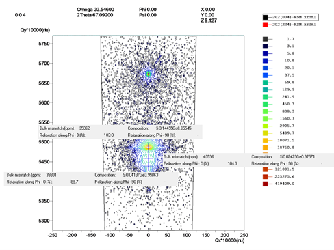
Figure 16. The RSM results show that the closer the SiGe layer is to the Si substrate, the smaller the lattice mismatch; the farther away from the Si substrate, the larger the lattice mismatch of the SiGe layer, resulting in a relaxation phenomenon of SiGe, that is, stress release. (Source: TSRI)
Example Six: Residual Stress Analysis of Polycrystalline Films
With the development of 3D packaging technology, under the complex stacking of materials and through multiple different processes, internal stress is likely to occur between layers due to differences in film thickness or material properties, such as thermal expansion coefficient, density, lattice spacing, etc. Subsequent processes, such as CMP grinding, may lead to delamination or cracking in areas of localized stress concentration, resulting in product failure. Therefore, in recent years, the semiconductor industry has gradually increased its awareness of thin film residual stress analysis.
When the film is subjected to compression or stretching, the lattice spacing of the material changes. Therefore, the change in lattice can be obtained by measuring the angular displacement of the diffraction peak (Δ2θ) using XRD or GIXRD (Figure 17). Based on solid elasticity theory, the residual strain of the film can be calculated, and by incorporating the material's Poisson's ratio and Young's modulus, the residual stress of the film can be determined (Figure 18).
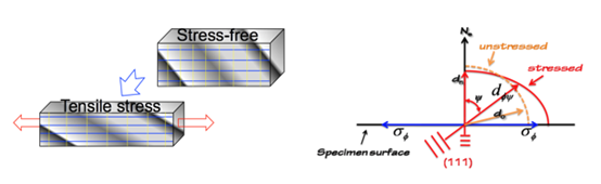
Figure 17. Schematic diagram of the change in lattice spacing in various directions under compression or tension.
Figure 18 shows the GIXRD analysis results of the Cu film. As the φ angle changes, it can be observed that the diffraction peak position gradually shifts to lower angles, indicating a change in lattice spacing, which suggests the presence of residual stress within the film, leading to different variations of the same lattice plane in different directions.
__26D20f59Eb.png "18 (1)")
Figure 18. The residual stress analysis results of polycrystalline Cu film, obtained through low-angle diffraction analysis to acquire Δ2θ, calculated the residual stress of the film to be 0.567 GPa tensile stress using elastic theory.
Electron microscopy and X-ray diffraction are two common tools for microstructure analysis of materials. Electron microscopy can observe the fine structure of specific areas, but it requires sample preparation and must be conducted in a vacuum testing environment. XRD analysis, on the other hand, can be performed in atmospheric conditions without special sample preparation, making it more convenient for analysis. Additionally, XRD is a non-destructive analysis method that can be conducted in situ under the sample environment, and by averaging results from large area analyses, the overall characteristics of the material can be obtained.
XRD technology can analyze the crystallographic phase, crystal orientation, crystallinity, grain size, optimal orientation of coatings, and residual stress analysis of polycrystalline films; when paired with high-resolution accessories, it can perform coating/epitaxial quality analysis, composition ratio of heteroepitaxial films, thickness, lattice matching, or relaxation analysis; using total reflection technology, it can analyze multilayer film thickness, surface/interface roughness, material density, etc. In summary, the application scope of XRD is very broad, providing considerable technical solutions for advanced processes or material development.


