
Failure Analysis
10.18
2024
The most important memory embedded in AI chips - Static Random Access Memory (SRAM) advanced process structure inspection and analysis.
AI chips and SRAM
The development of generative AI has brought about the Fourth Industrial Revolution. Through the increasing innovation of semiconductor heterogeneous integration in 3D packaging and node scaling technology, we witness the arrival of the AI era. The IC (Integrated Circuit) chips used in AI, also known as AI chips, are the hardware core of AI. TSMC's advanced logic technology has achieved over 20 billion transistors on a single chip, and it is expected that future products will reach over 1 trillion transistors through heterogeneous integration in 3D packaging. In such complex IC circuits, the heaviest embedded memory in AI chips is SRAM (Static Random-Access Memory). This embedded SRAM is also referred to as embedded SRAM. The importance of SRAM in embedded applications has two aspects: (1) SRAM is often the main memory cache (Register) and cache memory (Cache, also known as high-speed buffer storage) that constitutes the fastest read and write in AI chips. (2) Moreover, the process structure of SRAM is usually the smallest size and most densely packed area in AI chip processes. Because of its small size, more memory can be accommodated within the same chip area, thus reducing relative costs, making the status of SRAM in AI chips self-evident. The most advanced AI chips use process nodes that have entered the 3nm process, with products of 2nm and 16A (angstrom) process nodes expected to be launched in 2025 and 2026, respectively. SRAM will still be the most important memory in AI chips. Therefore, analyzing the structures of advanced process SRAM remains an important topic.
The circuit structure of SRAM
SRAM, also known as Static RAM (Random-Access Memory), is a type of random-access memory. The term "static" refers to the fact that this type of memory can maintain stored data as long as power is supplied. When the power supply is interrupted, the data stored in SRAM will still disappear (referred to as volatile memory), which is different from ROM (read-only memory) or Flash Memory that can retain data after power loss.
The circuit structure of SRAM can have different designs based on the number of transistors, such as 4T/6T/8T/12T, etc. The 6T design is the most commonly used SRAM design, where the T in 6T stands for Transistor. 6T indicates that the SRAM consists of 6 MOS (Metal Oxide Semiconductor) transistors as a basic unit. The circuit and component names of 6T SRAM are shown in Figure 1. Among the 6 transistors, there are 2 PMOS and 4 NMOS. The 6 transistors can be categorized into different functional components such as PU (Pull Up), PD (Pull Down), and PG (Pass Gate) based on their circuit functions.
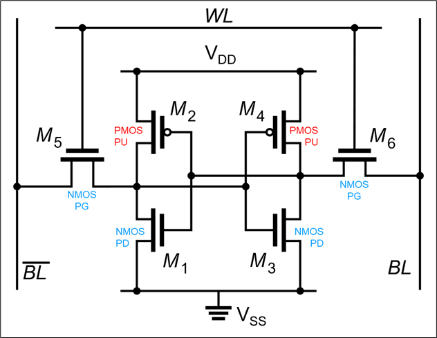
Figure 1: The circuit of 6T SRAM and the names of each part. (Reference [1])
WL: Word Line, Character Line
BL: Bit Line
First layer metal interconnect (signal transmission)
M2~M6: Follow M1 analogy
PU: Pull Up, pull-up transistor
PD: Pull Down, Pull Down Transistor
PG: Pass Gate, Transmission Gate Transistor
VDD: D=device, meaning the device, which refers to the operating voltage inside the device.
VSS: S=series, indicating a common connection, usually referring to the voltage of the circuit's common ground terminal.
Common detection and analysis methods for embedded SRAM areas
There are many commonly used AI chip testing and analysis methods, which can be roughly divided into Electrical Testing, Electrical Failure Analysis (EFA), and Physical Failure Analysis (PFA). PFA includes Surface Analysis and Chemical Analysis (CA). If we compare it to medical center examinations, Electrical Testing is equivalent to a health check-up, and so on, as shown in Figure 2. There are numerous testing and analysis methods commonly used in the embedded SRAM area, and this article will further explore the observation and analysis of SRAM structures.
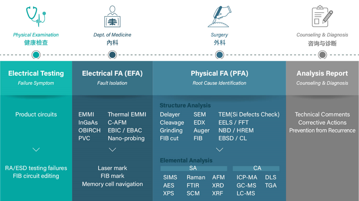
Figure 2 Comparison of Medical Center Testing and IC Testing Analysis
SRAM process structure observation tools
The main observation tools for SRAM structures include OM (Optical Microscope), SEM (Scanning Electron Microscope), DB-FIB (Dual Beam Focused Ion Beam), and TEM (Transmission Electron Microscope). These analytical devices can observe the SRAM process structures in AI chips, but their observation ranges are different, as shown in Figure 3. The selected method is to first use OM for large area observation, usually to find the approximate location of the target area on the chip. Then, SEM or FIB is used to narrow down the target area to a smaller region. FIB combined with SEM can provide precise positioning observation, and FIB is also an important tool for preparing TEM samples. If SEM/FIB cannot clearly observe the final target, TEM or Cs-TEM is used last. TEM can observe nanoscale small area structures. Cs-TEM (spherical aberration corrected TEM) is currently the device that can achieve a spatial resolution of 0.5Å (angstrom, 10 billion angstroms = 1 meter), meaning Cs-TEM has the highest magnification capability available. Additionally, SEM and TEM can be combined with EDS (Energy-dispersive X-ray spectroscopy) to analyze the composition of small areas.
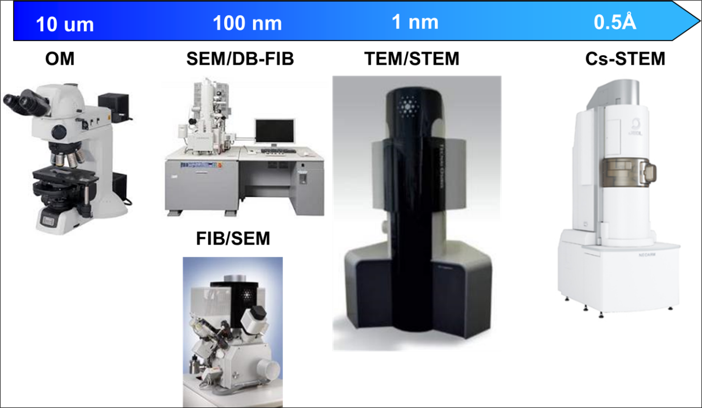
Figure 3 OM/SEM/TEM and Observation Range
How to find embedded SRAM areas in AI chips
Since SRAM is the smallest size and densest area in AI chip processes, and memory is usually arranged repetitively, using these two characteristics to identify SRAM areas has certain feasibility and reliability. Figure 4 shows the use of OM to observe the chip and identify the approximate range of embedded SRAM areas. Some SRAM areas are indicated by the blue box. Finding the approximate areas of SRAM helps in further detailed electrical size and physical property analysis.
In addition to OM, IR (Infrared) microscopes and SEM are also commonly used tools for extensively searching for embedded SRAM areas. The method for identifying the range of embedded SRAM areas is the same as that for OM. However, SEM is a relatively easier method to confirm SRAM, as OM has a smaller magnification and may sometimes be unclear.
__26D20syyJj.png "4 (1)")
Figure 4 shows the area of the embedded SRAM region of the chip observed using OM. Some SRAM areas are indicated by the blue box.
Applications of SEM and VC
SEM is a type of electron microscope that generates images of the sample surface by scanning it with a focused electron beam, typically observing structures larger than 100nm. SEM has many applications. The primary use of SEM is to observe the surface structure of samples. Additionally, SEM combined with nano-probing can perform electrical measurements, which will not be discussed in this article. SEM combined with FIB (Focus Ion Beam) is referred to as DB-FIB, which will be discussed in the next chapter. Here, we will introduce VC (Voltage Contrast). The VC positioning technique utilizes the primary electron beam or ion beam from SEM or FIB to scan the sample surface. Different areas of the chip surface have different electric potentials, and after SEM scanning, different regions of the sample or specimen surface exhibit varying brightness contrasts, which is referred to as VC. The principle of VC can be referenced in the literature [2].
SRAM includes PMOS and NMOS regions. Under specific voltage operations, VC effects are usually observed during SEM scanning of the IC's vias or contact windows. At low voltage operations, the brightness of the vias/contacts in the PMOS region observed by SEM is the brightest, followed by the NMOS region, and if there are structural positions in the gate level vias/contacts, this area appears the darkest. Figure 5 shows the different brightness contrasts caused by SEM scanning in the contact area of SRAM.
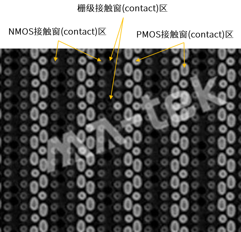
Figure 5 SEM scanning causes different brightness contrasts in the contact area of SRAM.
DB-FIB is a precision positioning cutting device.
The Focus Ion Beam (FIB) microscope uses gallium (Ga) metal as the ion source, with a melting point of 29.76°C and a vapor pressure of «10-13 Torr, making it suitable for operation under vacuum. During use, the liquid gallium flows along the filament to the tip, and when the applied electric field is strong enough to pull the liquid gallium at the tip into a conical shape with a curvature radius smaller than a critical radius (Taylor cone), gallium is ionized and ejected, forming a gallium ion beam. This ion source has a size smaller than 10 nm, an energy dispersion of about 4.5 eV, and a brightness of about 106 A/cm2.sr, making it a very precise tool for nanostructure processing, also referred to as a nanoscopic sculpting tool. Additionally, an electron beam system can be installed on the FIB microscope, forming what is known as a Dual Beam FIB, which combines a scanning electron microscope (SEM) and a Focus Ion Beam (FIB) in one system. It can use the electron beam to locate target areas and observe images, while the ion beam performs precise cutting of the target area without damaging other sample structures; thus, it can achieve nanometer-level precision in positioning and cutting, as well as in the preparation of TEM sample thin sections. The DB-FIB machine can be referenced in Figure 3. The relative position diagram of the DB-FIB's SEM (E-beam) and FIB (i-beam) to the sample is shown in Figure 6. Figure 7 illustrates the precise positioning and cutting using DB-FIB, observing the cross-sectional structure of SRAM. In the figure, both the front-end-of-line (FEOL) and back-end-of-line (BEOL) process areas can be observed.
-
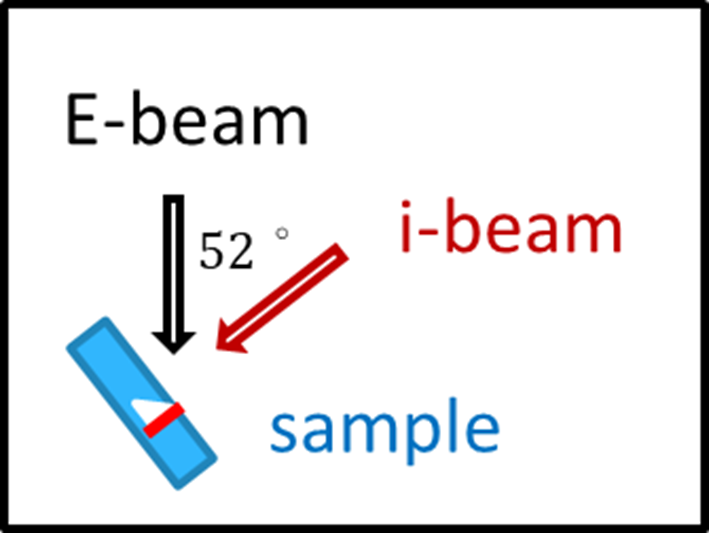 Figure 6 is a schematic diagram of the relative positions of DB-FIB's SEM (E-beam) and FIB (i-beam) with the sample.
 -
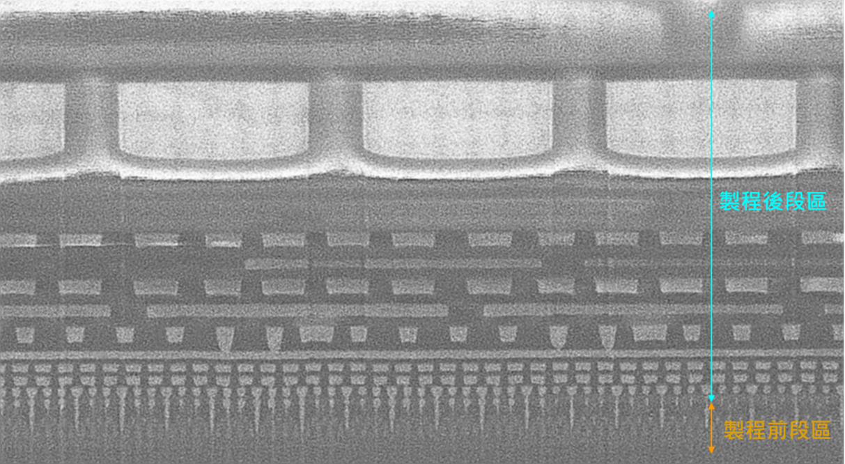 Figure 7 Using DB-FIB for precise cutting and observing the cross-sectional structure of SRAM.
TEM is an important method for observing the SRAM manufacturing process layers.
To observe the component structure and fine process levels of advanced 6T SRAM technology, it is necessary to use TEM (Transmission Electron Microscope) or STEM (Scanning Transmission Electron Microscope) to see clearly. TEM utilizes a 200KV accelerated electron beam to penetrate thin samples (approximately 100nm thick or smaller) and projects the signals onto a detector, which are presented as images. For today's 3nm process or mature processes, as well as future 2nm and 16A (angstrom) process nodes, TEM has always been the most important inspection and analysis method for observing SRAM structures, because TEM has the best spatial resolution and image presentation.
The circuit and component names of the 6T SRAM seen in Figure 1 can be clearly observed in their true structure using TEM. Figure 8 shows a plan-view STEM observation of the advanced process 6T SRAM, where the planar structure of the six transistors and their relative arrangement can be seen, including the planar arrangement of the Contact, Gate, Fin, STI, and other front-end process structures. The yellow box in Figure 8 represents one unit cell of the 6T SRAM. Figure 9 shows a cross-section (XS) TEM observation of part of the transistor structure of the advanced process 6T SRAM, where the shape structure of the transistors arranged vertically can be seen, including the cross-sectional arrangement of the Contact, Gate, Fin, STI, and other front-end process structures.
-
__26D20wflY3.png "8 (1)") Figure 8 Plan-view Transmission Electron Microscope (TEM) observation of advanced process 6T SRAM, the yellow framed area is the 1 unit cell of 6T SRAM.
Figure 8 Plan-view Transmission Electron Microscope (TEM) observation of advanced process 6T SRAM, the yellow framed area is the 1 unit cell of 6T SRAM. -
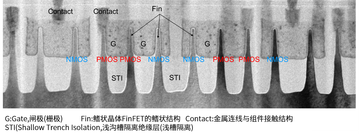 Figure 9 Cross Section (XS) Transmission Electron Microscope (TEM) observation of the transistor structure of 6T SRAM in advanced processes.
Conclusion
The observation of SRAM structures is an important part of the detection and analysis of AI chips. This article demonstrates step-by-step methods for observing SRAM structures using OM, SEM, TEM, etc. It mainly starts with wide-range low-magnification OM observations and goes up to the highest magnification and smallest range TEM, introducing the important structures and names of SRAM through images and text, achieving effective and precise observation methods for SRAM structures.
MA-tek provides you with the most advanced AI chip testing and analysis.
MA-tek is the world's leading semiconductor analysis laboratory. It has the largest and most comprehensive materials analysis, failure analysis, and reliability analysis equipment in the world. Its technical capabilities can analyze not only the most advanced IC processes currently available but also the analysis capabilities for more advanced processes and components in the next 5 to 10 years or beyond.
Reference:
[1] https:// zh.wikipedia.org/zh-tw/靜態隨機儲存器
[2] V.G. Dyukov, S. A. Nepijko, Gerd Schoenhense, Voltage Contrast Modes in a Scanning Electron Microscope and Their Application, August 2016, Advances in Imaging and Electron Physics.


