
Silicon photonics technology: Opening the door to the future of high-speed optical communication.
Silicon Photonics: Opening the Door to the Future of High-Speed Optical Communications
Professor Guo Haozhong's team
National Yang Ming Chiao Tung University, Department of Photonics Engineering
-
1. Introduction

With the expansion of data centers, the development of artificial intelligence, and the rise of 5G and 6G communication technologies, the global demand for high-speed data transmission is increasing. Traditional electronic components have approached their limits in speed and energy efficiency, thus "Silicon Photonics" has become the focus of industry attention. Silicon photonics utilizes silicon materials to manufacture optical components, making them compatible with existing semiconductor processes, providing efficient, low-power, and mass-producible optical solutions.
Silicon photonics applications cover areas such as data centers, telecommunications, LiDAR, autonomous driving, medical imaging, quantum computing, and high-performance computing. These applications are all connected to the central silicon photonics chip, symbolizing its core role in various technologies.
2. Overview of Silicon Photonics
Why use silicon for optical communication transmission instead of other materials?
Figure 2 lists different materials used for optical communication transmission compared to silicon. Taking III-V materials InP as an example, the advantage is that it can directly integrate light sources without the need for additional external light source coupling and packaging, but the disadvantage is that the current process for this material is below 4 inches, with low yield and high cost. If glass is used, the advantages are low cost and easy material acquisition, while the disadvantages are unstable process yield and the technology still needs to be developed. Finally, there are polymer materials, whose advantages are low cost and fast processing, but the disadvantages are poor reliability, difficult quality control, and susceptibility to deformation, which can affect high-frequency transmission.
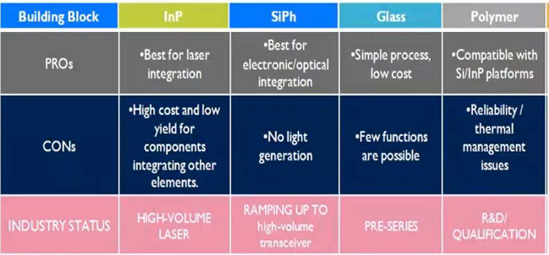
Figure 2. Comparison of Optical Communication Waveguide Transmission Materials
Silicon photonics technology refers to the use of silicon as the base material to manufacture optical components, enabling the transmission, modulation, detection, and processing of optical signals. Unlike traditional electronic signals, optical signals can transmit data at higher speeds while reducing power consumption, which makes silicon photonics play a key role in high-performance computing and high-speed networks.
The core advantages of silicon photonics technology include:
- High-speed transmissionThe bandwidth of optical signals is much greater than that of electronic signals, reaching hundreds of GHz or even higher.
- low energy consumptionThe energy loss during optical signal transmission is lower, which can reduce heat generation and power consumption compared to electronic transmission.
- high integrationSilicon photonics technology can be compatible with existing CMOS processes, achieving the monolithic integration of electronic and photonic components.
- scalabilityIt can be mass-produced through existing semiconductor processes, reducing production costs.
3. Key Technologies of Silicon Photonics
The core components of silicon photonic systems include active components (such as lasers, modulators, and detectors) and passive components (such as waveguides, couplers, and beam splitters), where waveguide components are responsible for the transmission and manipulation of optical signals. The core technologies are described as follows:
- Active components:
- Laser light source: Usually a high power (>40mW) Distributed Feedback Laser with wavelengths in the O-band and C-band, serving as a laterally emitting light source.
- Optical detector: Ge-doped optical detector, usually at the receiving end Rx, converts the optical signal received from the output end Tx into photoelectric current, which is then processed into a signal by chips such as TIA.
- Optical modulator: By controlling the modulator through RF power, it creates changes that allow light to produce a switching effect, generating high-frequency digital signals as the speed increases.
- Passive components:
- Mux/Demux: Usually for medium to long distance transmission, used for wavelength division multiplexing and mixed light purposes, mainly for processing different wavelengths of multimode light.
- Coupling I/O: Optical coupling, introducing external light sources into silicon photonic components, is divided into Edge coupling, Grating coupling, and V-groove coupling.
- Optical filter: used for medical inspection applications.
- Interferometer/Switch: Modulates the phase of light and adjusts the direction of light.
- Splitter/Combiner: Mainly used for splitting single-mode optical signals into multiple outputs or combining multiple optical signals, optical power distribution, and direction adjustment.
- Polarization Diversity: Polarization control, the propagation characteristics of TE (Transverse Electric) and TM (Transverse Magnetic) modes are different, which may lead to certain devices being suitable only for specific polarization states, such as MZI modulators and optical couplers primarily supporting TE mode, while TM mode may not be able to transmit effectively.
- Waveguide: The main path for light in silicon photonic chips, abbreviated as optical path, equivalent to the circuit function in IC.
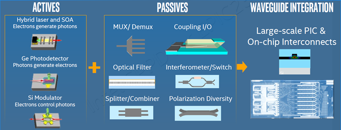
Figure 3. The components of silicon photonic devices are divided into active structures, passive structures, and waveguide structures (Intel)
2.5D packaging is a technology that lies between traditional 2D packaging (chips on a flat circuit board) and 3D packaging (multi-layer chip stacking). It mainly uses a silicon interposer to place multiple chips (such as processors, memory, etc.) on the same plane, and enhances performance through Through-Silicon Vias (TSV). Combining silicon photonic components to create optoelectronic integrated modules reduces losses by transmitting some high-speed electrical signals as optical signals, achieving high-speed transmission.
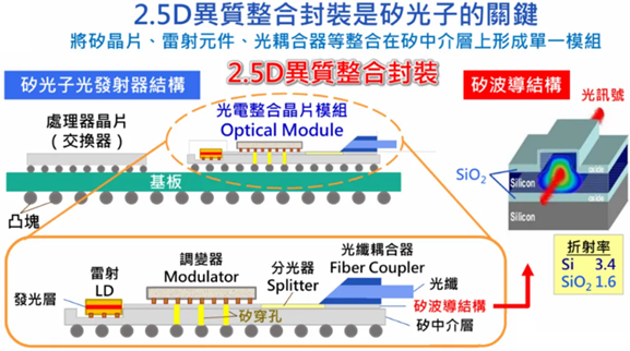
Figure 4. Basic optical components in a 2.5D packaging system, including laser light source, modulator, demodulator, micro-ring resonator, and optical waveguide.
- Optical modulation technology
Optical modulation is one of the core functions in silicon photonics technology, determining how to effectively convert electronic signals into optical signals. Common optical modulation techniques include:
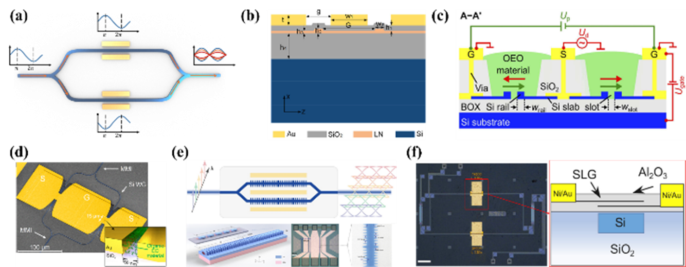
Mach-Zehnder Modulator (MZM)
- Mainly consists of two waveguides, one of which changes its refractive index when voltage is applied, causing a change in the phase of the light wave. When the two beams of light combine, constructive and destructive interference occurs, resulting in the effects of light transmission and absorption, thereby modulating the optical signal.
- Advantages: high linearity, large bandwidth, suitable for high-speed transmission.
- Challenges: Occupies a larger area and has higher power consumption.
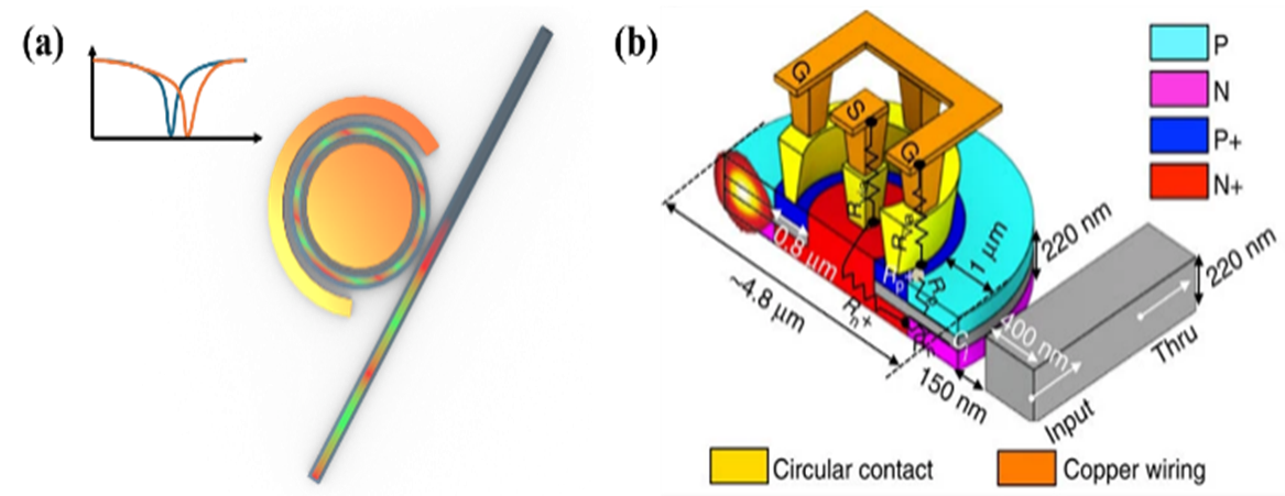
Microring/Microdisk Modulators (MRM/MDM)
- Using micro-ring resonators to modulate optical signals, which are small in size and highly efficient. RF signals are used to modulate the control of light entering the waveguide, resulting in absorption and transmission through the Ring to generate signal modulation.
- Advantages: low power consumption, large-scale integration.
- Challenge: Sensitive to process variations and temperature changes.

Ring-Assisted Mach-Zehnder Modulator (RAMZM)
- Combining the advantages of ring resonators and MZMs enhances modulation performance. Micro-ring resonators can produce larger phase changes with smaller electric field variations, thus the RA-MZM can significantly reduce driving voltage compared to traditional MZIs, thereby lowering power consumption.
- Advantages: Enhance modulation depth, reduce insertion loss.
- Challenge: The process and design are more complex.
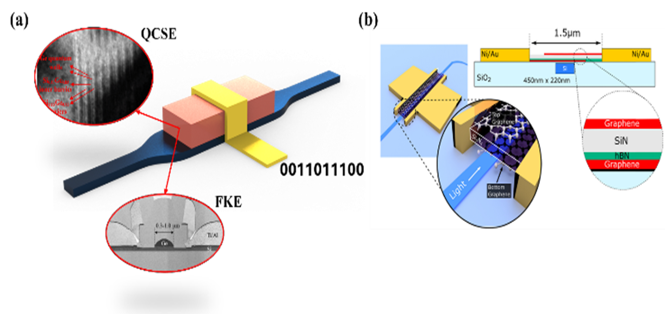
Electro-Absorption Modulator (EAM)
- Through the Quantum Confined Stark Effect (QCSE), the absorption characteristics of the material are modified under the influence of an electric field to modulate light intensity.
- Advantages: small size, low power consumption, suitable for high-speed transmission.
- Challenge: Optical loss is relatively large, requiring optimization of material properties.。
2. Optical modulation mechanisms in silicon photonics
Optical modulators change the properties of light through various physical mechanisms to achieve high-speed data transmission. The following are several main modulation mechanisms:
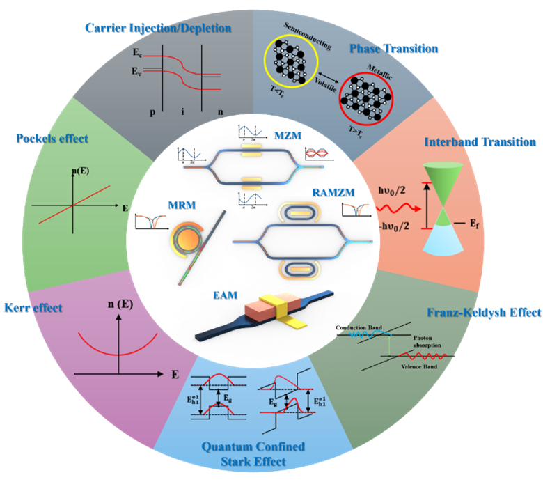
- Plasma Dispersion EffectBy adjusting the concentration of free charge carriers, the refractive index and absorption rate of the material can be changed.
- Pockels effectUsing an external electric field to change the refractive index of non-centrosymmetric materials.
- Franz-Keldysh effectWhen an external electric field changes the energy band structure of a semiconductor, it extends its absorption edge, allowing photons with energy below the bandgap to be absorbed.
- Quantum Confined Stark Effect (QCSE)Enhance the effect of the electric field on the band structure through quantum well structures.
- Slow light effectBy reducing the group velocity of light within the photonic structure, the interaction between light and matter is enhanced, effectively extending the interaction time without increasing the length of the device.
- Band gap transitionBy changing the energy states of electrons to influence the absorption and refraction of light.
- Phase change effectThe refractive index undergoes a dramatic change when the material transitions between crystalline and amorphous states.
3. Silicon Photonic Detector
Photodetectors (PD) are responsible for converting optical signals back into electronic signals and are an indispensable component of silicon photonics technology. Common technologies include:
- Ge/Si photodetectorUtilizing the light absorption characteristics of germanium, integrated with silicon chips, to achieve high-performance detection.
- Graphene PhotodetectorUtilizing the high carrier mobility and broad bandwidth absorption characteristics of graphene to achieve ultra-high-speed detection effects.
4. Silicon photonic waveguides and optical connections
- Waveguide technologySilicon photonic waveguides can guide optical signals to different components, enhancing overall system performance.
- Optical InterconnectSilicon photonics can be applied in data centers and supercomputers to reduce transmission latency and power consumption.
4. Applications of Silicon Photonics
High-speed optical communication
The main application of silicon photonics technology is high-speed optical communication, for example:
- Data center interconnect: Utilizing silicon photonics technology to enhance data transmission speed between servers.
Fiber to the Home (FTTH): Enhancing the performance of fiber optic networks through silicon photonic modules.
Satellite and Space Communication: Silicon photonics technology can be used for optical laser communication, enhancing long-distance transmission capabilities.
High Performance Computing (HPC)
- Artificial Intelligence and Machine Learning: Silicon photonics technology can accelerate data transmission and improve AI computing performance.
- Quantum Computing: Silicon photonics technology is used to develop quantum optical computing platforms.
3. Biomedical and Sensing Technology
- Optical biosensors: Silicon photonic biosensors can be used for disease diagnosis, such as COVID-19 virus testing.
- Environmental monitoring: Using optical sensors to detect air and water quality pollution.
5. The Future Development of Silicon Photonics
- Increase modulation speed and bandwidth
- Research new materials, such as silicon nitride and lithium niobate (LiNbO₃), to enhance optical modulation performance.
- Reduce power consumption and the impact of thermal effects
- Using new technologies such as graphene and photonic crystals to reduce power consumption and temperature variation.
- Deep integration of photons and electrons
- Develop silicon photonic chips, closely integrating with existing electronic components to enhance overall computing performance.
- Emerging application expansion
- Further promote the application of silicon photonics technology in fields such as biomedicine, smart sensing, and quantum communication.
6. Conclusion
Silicon photonics technology is rapidly developing, driving innovations in optical communication, computing, and sensing technologies. By continuously improving modulation efficiency, reducing power consumption, and enhancing integration, silicon photonics will become one of the key technologies for future digital infrastructure. In the future, with advancements in process technology and materials science, silicon photonics technology will further expand its application scope, changing the way we communicate and compute. As data volumes grow exponentially, the demand for high-speed optical modulators in modern optical communication networks is increasing. The table below summarizes the performance, advantages, and challenges of different types of modulators in silicon photonics technology, helping to choose the most suitable modulation technology based on application needs.
| Parameter |
Mach-Zehnder Modulator (MZM) |
Ring Modulator (Ring Modulator) |
Ring-Assisted Mach- Zehnder Modulator (RAMZM) |
electro-absorption modulator (EAM) |
|---|---|---|---|---|
|
bandwidth (GHz) |
Max >110 GHz Standard: 30–110 GHz |
Max >77 GHz Standard: 30–77 GHz |
Max: 58.5 GHz Standard: 8.5–58.5 GHz |
Max: 89 GHz Standard: 26.8–89 GHz |
|
Voltage-length product (Vπ·L) |
Min. : 0.003 V·cm Standard: 0.003–1.6 V·cm |
Min. : 0.52 V·cm Standard: 0.52–0.8 V·cm |
Min. : 0.025 V·cm Standard: 0.025–1.73 V·cm |
No specific applicable data |
|
Extinction ratio (ER, dB) |
Max: >50 dB Standard: 3.15–50 dB |
Max: 25 dB Standard: 3.5–25 dB |
Max: 30 dB Standard: 8–30 dB |
Max: 14.15 dB Standard: 3–14.15 dB |
|
Insertion Loss (IL, dB) |
about 1.7 dB to 18 dB, Depends on the device length and materials |
less than 2, 0.7 dB to about 14 dB, Usually lower |
2 dB to 10.5 dB,Depending on the design complexity |
1.8 dB to 6.2 dB,Affected by material absorption |
|
Device size |
Length approximately 0.12 mm to 3 mm, occupying a larger area. |
radius of approximately 3.7 µm to 15 µm,extremely compact |
Area of approximately 80×60 µm² to larger structures,Including ring and interferometer |
Dimensions approximately 40×0.3 µm², Simple and compact structure |
|
data rate (Gb/s) |
Max: 560 Gb/s Standard: 80–560 Gb/s |
Max: 330 Gb/s Standard: 128–330 Gb/s |
Max: 320 Gb/s Standard: 12–320 Gb/s |
Max: >112 Gb/s, Standard: 32–112 Gb/s |
|
Advantages |
High linearity, large bandwidth, suitable for long-distance transmission; hybrid integration can enhance performance. |
Compact size, high speed, low power consumption,Suitable for high-density integration applications |
Better extinction ratio and bandwidth,Achieving a balance between insertion loss and bandwidth |
High modulation efficiency, low power consumption,Compatible with CMOS;Graphene integration expands the spectrum range of accessories. |
|
Challenge |
Silicon MZM bandwidth is limited, Hybrid material device manufacturing is complex. |
the trade-off between speed, power consumption, and thermal stability,Sensitive to manufacturing errors |
The design and manufacturing processes are more challenging,Due to the need to integrate both the ring and the interferometer. |
The challenge of contact resistance in graphene devices;Need to balance speed and energy efficiency |
|
Common materials |
Silicon, Lithium Niobate (LiNbO₃), Silicon-organic hybrid materials |
SOI (Silicon On Insulator), Silicon Nitride (SiN), Hybrid materials |
InP (Indium Phosphide) thin film, SOI built-in micro-ring structure |
germanium (Ge), silicon-germanium (SiGe) quantum wells,Graphene-Silicon Hybrid Structure |
|
Typical applications |
Long-distance communication, data centers, high-capacity networks |
Chip internal interconnect, data center,Compact Modulation Applications |
High-Performance Radio Frequency Photonics,Applications requiring high extinction ratio and bandwidth |
data centers, telecommunications,Fiber Optic Wireless Communication,High-speed optical detection |


