
Introduction to Electrostatic Discharge Protection Technology for Gallium Nitride Chips
Introduction to Electrostatic Discharge Protection Technology for Gallium Nitride Chips
Professor Ko Ming-Tao, Doctoral Student Ko Chao-Yang
National Yang Ming Chiao Tung University, Institute of Electronics
-
-
Introduction to Gallium Nitride (GaN) Semiconductors and Their Market Applications
Gallium Nitride is a compound semiconductor composed of nitrogen and gallium elements, with a bandgap of 3.39 eV, which is wider than that of silicon (1.12 eV), as shown in Table 1. Therefore, Gallium Nitride semiconductors belong to the category of wide bandgap semiconductors. Due to the special characteristics of the wide bandgap that can provide a higher breakdown electric field, Gallium Nitride semiconductors are suitable for high power applications, such as renewable energy systems, power conversion systems, electric vehicles, data centers, compact chargers, etc. Since Gallium Nitride devices utilize a two-dimensional electron gas (referred to as 2DEG) as the channel switch, as shown in Figure 1, this 2DEG mechanism can achieve higher electron mobility, allowing for the fabrication of high electron mobility transistors (referred to as HEMT), which is beneficial for high-frequency applications in communication devices. Additionally, since Gallium Nitride has better radiation resistance compared to silicon, Gallium Nitride semiconductors can also be applied in aerospace devices, low Earth orbit satellites, etc. Due to the broad market applicability of Gallium Nitride, Gallium Nitride semiconductor devices and integrated circuits are currently one of the main semiconductor technologies being developed in the market.
| Characteristics | Si | SiC | GaN |
|---|---|---|---|
| bandgap (eV) | 1.12 | 3.26 | 3.39 |
|
Breakdown Electric Field (MV/cm) |
0.3 | 3.0 | 3.3 |
|
electron mobility (cm2/V-s) |
1450 | 900 | 2000 |
|
Saturation Drift Velocity (cm/s) |
107 | 2.2 × 10⁷ | 2.5 × 10⁷ |
|
Thermal conductivity (W/cm-K) |
1.5 | 4.5 | 1.3 |

Figure 1, Band diagram of Gallium Nitride devices and their two-dimensional electron gas.
2. The Importance of Electrostatic Discharge Events and Electrostatic Discharge Protection
Electrostatic discharge (ESD) is a naturally occurring phenomenon of charge discharge, which is more likely to occur when the humidity in the air is low. Therefore, in drier environments or during cold winter days, people often experience static electricity shocks. Although the human body can withstand the brief pain caused by electrostatic discharge, the instantaneous high current energy can potentially cause permanent damage to electronic products, especially for extremely small components like integrated circuits, which are particularly vulnerable. Therefore, the electrostatic discharge protection capability of electronic products directly affects their qualification rate and reliability, which is a crucial issue for wide bandgap semiconductors used in high-end electronic products such as electric vehicles, aerospace devices, and high-power devices. Figure 2 shows a common model in electrostatic discharge events, the human body model (HBM) equivalent circuit model. This model is used to simulate the electrostatic discharge event caused when a person with static electricity touches an integrated circuit product. The 100 pF capacitor simulates the equivalent capacitance of the human body, while the 1.5 kΩ resistor simulates the equivalent resistance of a human finger. When the switch is shorted to point A, the high-voltage source charges this capacitor to accumulate static charge. When the switch is shorted to point B, the accumulated static charge discharges through the resistor to the device under test (DUT). When this capacitor is charged to 2 kV, the current waveform generated during discharge to the DUT is shown in Figure 3. It can be observed that the peak current during discharge reaches up to 1.3 A, with a duration of about several hundred nanoseconds. This extremely high current generated in a very short time is particularly likely to damage integrated circuits. Since integrated circuit products may face electrostatic discharge events during the manufacturing process, it is necessary to design electrostatic protection mechanisms when designing integrated circuits.
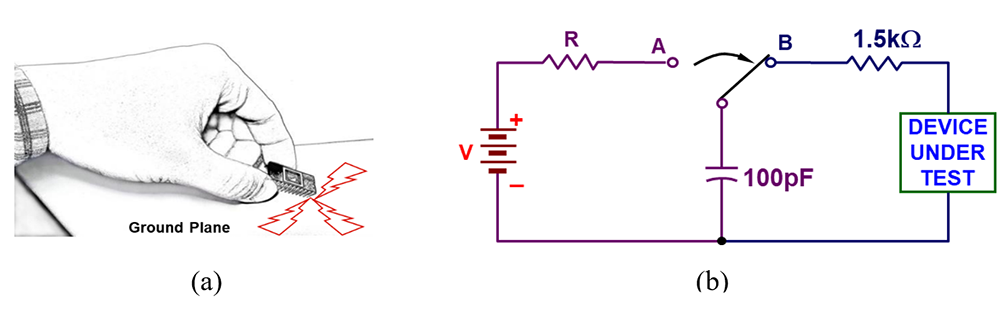
Figure 2, (a) Human discharge mode and (b) its equivalent circuit model.
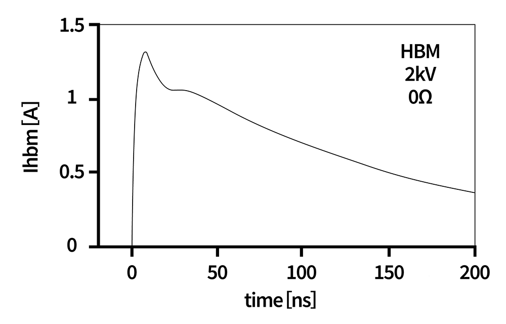
Figure 3, discharge current waveform of the HBM model with a cumulative 2-kV electrostatic discharge.
When designing electrostatic discharge (ESD) protection for integrated circuits, the concept of whole-chip ESD protection needs to be introduced to enhance the tolerance of integrated circuits under various electrostatic tests. In addition to designing protective components for input/output pins to conduct electrostatic current to VDD (system power) or VSS (system ground) pins, it is also necessary to design a power-rail ESD clamp circuit between VDD and VSS to provide an appropriate discharge path for electrostatic surge currents flowing from input to output. Therefore, when designing ESD protection for integrated circuits, it is usually necessary to consider the entire chip architecture comprehensively in order to optimize the design and enhance the ESD protection capability of the whole chip.
3. Investigation of Electrostatic Discharge Tolerance Characteristics of Gallium Nitride Devices and Component-Level Electrostatic Protection Design
3.1 Investigation of Electrostatic Discharge Tolerance Characteristics of Gallium Nitride Devices
In recent years, due to the increasing research on Gallium Nitride, the electrostatic tolerance characteristics of GaN devices and the design of electrostatic discharge protection at the device level have been proposed. Regarding the electrostatic tolerance characteristics of GaN devices, studies have found that the gate and source exhibit poorer electrostatic tolerance. The device measured in Figure 4 is a metal insulator semiconductor (HEMT) with a total channel width of 120,000 μm. As shown in the experimental results of Figure 4, it can be observed that except for the GS +/- HBM mode (where electrostatic testing is applied from the gate pin and the source is grounded) which has an electrostatic tolerance of less than 2 kV, all other test modes are above 2 kV. Further failure analysis confirmed through Optical Beam Induced Resistance Change (OBIRCH) indicates that the failure location of the device under the GS - HBM mode is between the gate and source, as shown by the red highlight in Figure 5. Observations of the device were made using a Scanning Electron Microscope (SEM) and a Focus Ion Beam Microscope (FIB), as shown in Figure 6(a). Further analysis of the structural cross-section at points A/B reveals that the normal structure between the gate and source is as shown in Figure 6(b), while Figure 6(c) shows severe damage in the insulation layer region. Therefore, even with an HBM impact energy of only -0.5 kV, it is sufficient to cause severe damage, leading to device failure.
-
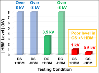
Figure 4, the HBM electrostatic tolerance of Gallium Nitride devices (MIS-HEMT) under various test modes [5].
-
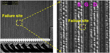
Figure 5, using OBIRCH analysis under GS-HBM mode, the failure location of the GaN HEMT device is located between the gate and source [5].
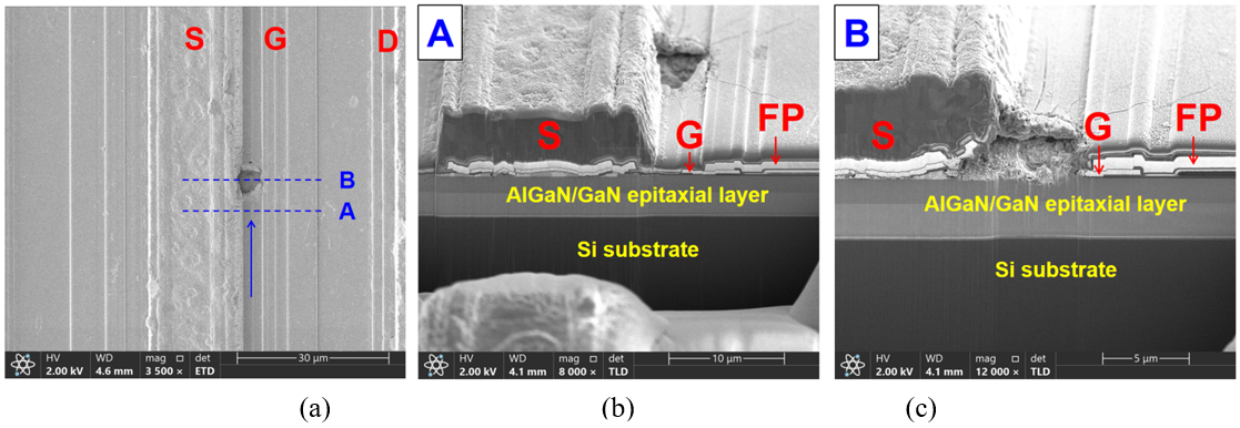
Figure 6, using SEM and FIB to analyze the GaN HEMT device under the GS-HBM model: (a) top view, (b) cross-section at point A, (c) cross-section at point B [5].
3.2 ESD Protection Design at the Device Level for Gallium Nitride Devices
Due to the poor electrostatic tolerance of Gallium Nitride (GaN) devices at the gate, discrete devices require specially designed electrostatic protection circuits for the gate. In recent years, several papers have discussed the design of electrostatic protection for the gate of GaN devices. Figure 7 shows the gate electrostatic protection circuit implemented using the over-voltage detection principle. When an electrostatic over-voltage occurs at the gate terminal, the over-voltage causes the diode to conduct, and the voltage drop across the resistor generated by the current flowing through will turn on the ESD HEMT. However, this solution requires additional photolithography to fabricate the diode, increasing the cost and difficulty of the process, and in practical applications, the gate terminal V.GThe voltage will be determined by the number of diodes in series, as the gate voltage VGwill be clamped at the forward voltage of the diode, and the diode will also have a leakage path that increases the circuit's power consumption. In addition, due to the GaN HEMT device, when turned off, it is necessary to set the gate voltage VGA negative voltage must be applied to turn it off, but the HEMT is a bidirectional device, meaning that as long as the ESD HEMT gate voltage VG,ESDGate voltage V of power HEMTGThe components can also conduct, making this design unable to support negative voltage applications.
Considering the shortcomings of the above design, an improved design has also been proposed in recent years[6]. Figure 8 presents the circuit diagram of this improved design, which operates primarily by stacking two HEMT devices (ESD HEMT1 and ESD HEMT2) to enable application in the case of negative gate voltage for the power device Power HEMT. When the gate of the Power HEMT is at a positive bias, the channel of ESD HEMT2 will be turned on, but the gate of ESD HEMT1 is connected to ground through resistor R3, thus remaining in the off state, preventing any leakage path between the G and S terminals. When the gate of the Power HEMT is at a negative bias, the channel of ESD HEMT1 will be turned on, but the gate of ESD HEMT2 is connected to the negative bias through resistor R2, thus remaining off, and there will also be no leakage path between the G and S terminals. When an ESD strike occurs at the G terminal, the C of ESD HEMT1.GDThe capacitance (the capacitance between the gate terminal and the drain terminal) will couple the electrostatic voltage to the gate of ESD HEMT1, causing the channel of ESD HEMT1 to turn on. At the same time, the channel of ESD HEMT2 will also turn on due to the coupling effect, and since the gate of ESD HEMT2 is connected to the G pin, its channel will also turn on due to the charging of the gate capacitance. Therefore, when electrostatic discharge occurs, it can ensure that both ESD HEMT1 and ESD HEMT2 transistors are turned on, thus providing a path for electrostatic discharge. It is worth mentioning that in addition to supporting applications with negative gate bias, this design does not require the use of diodes, thus avoiding additional photolithography and process costs, and there will be no diode leakage paths, thereby preventing additional power consumption of the chip.
-
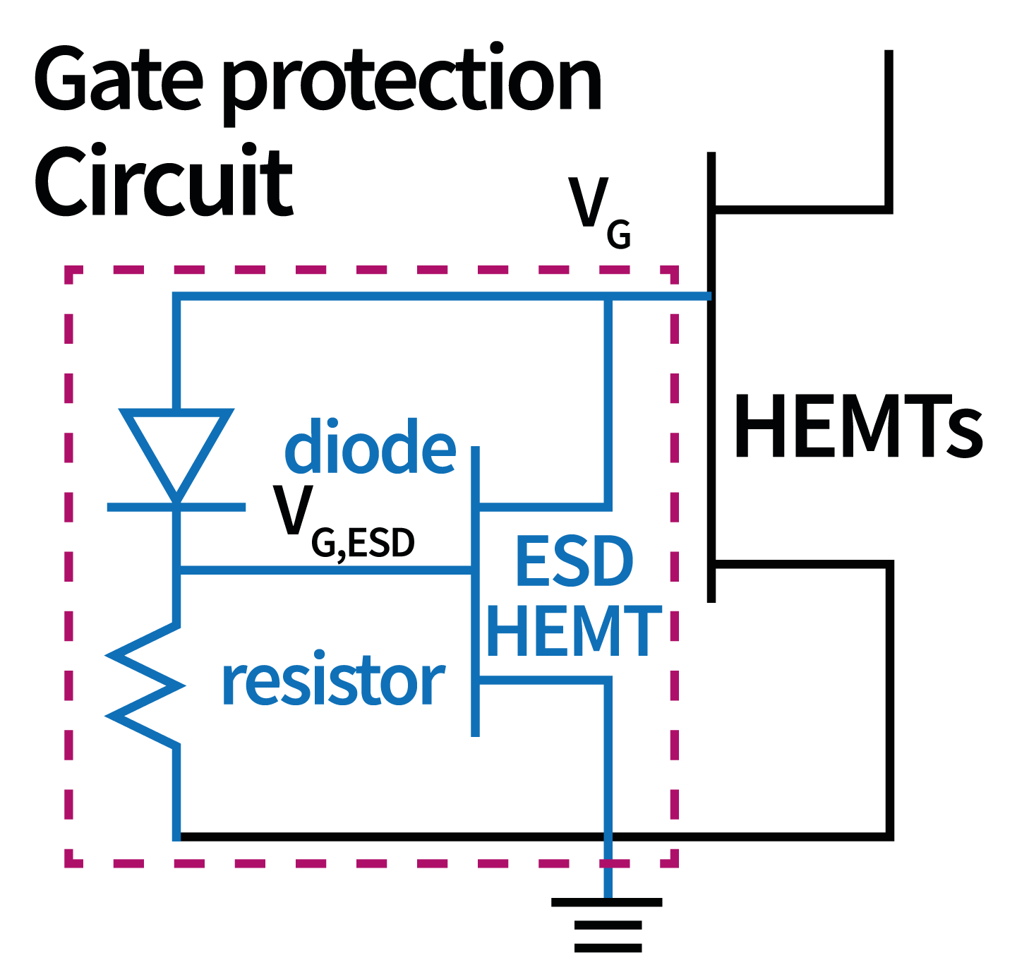
Figure 7, ESD protection circuit design for gate terminal of GaN HEMT discrete device.
-
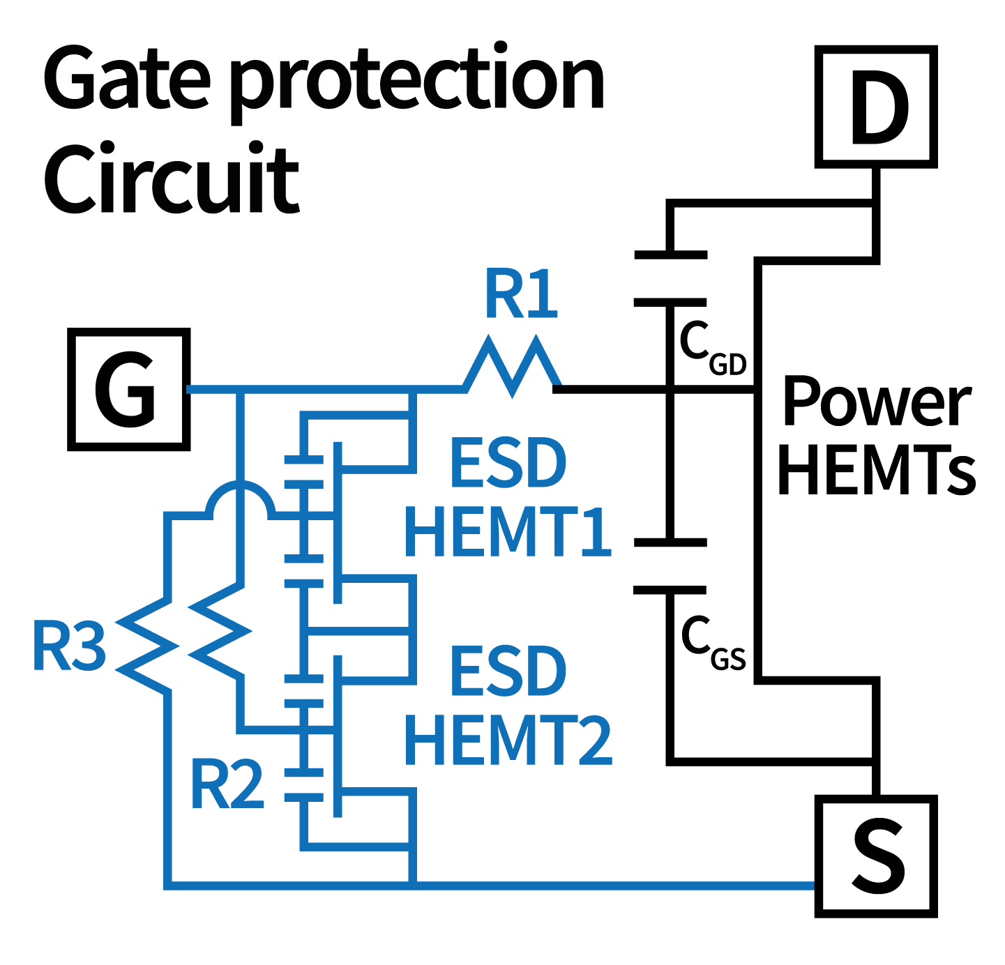
Figure 8, Improved Electrostatic Discharge Protection Circuit at the Gate Terminal of GaN HEMT Discrete Devices.
4. Design of Electrostatic Discharge Protection Circuits for Gallium Nitride Integrated Circuits
4.1 GaN Whole-chip ESD Protection Design Concept
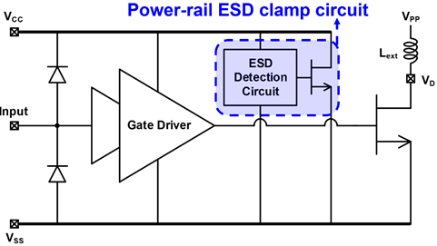
4.2 Power-rail ESD clamp circuit for Gallium Nitride (GaN) wafers
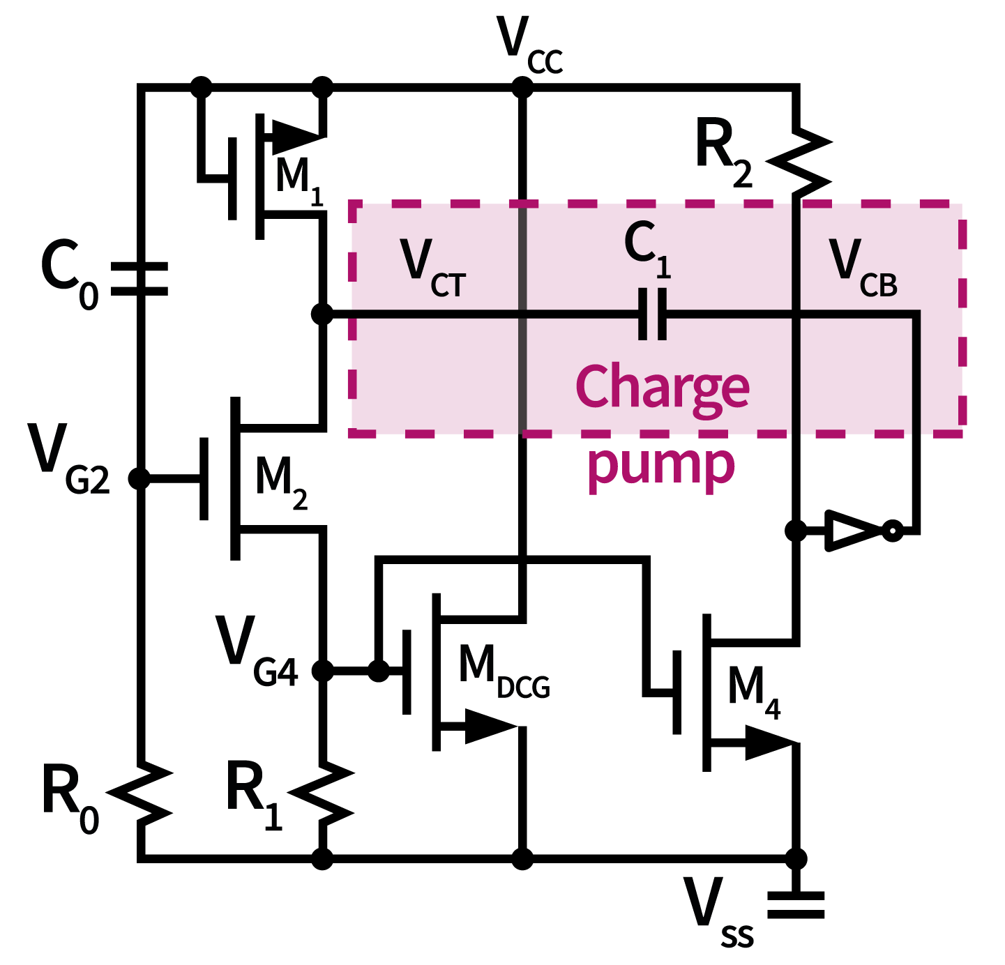
Due to the critical role that power-rail ESD clamp circuits play in enhancing the electrostatic discharge protection capability of the entire chip, several papers have explored the design of power-rail ESD protection circuits for Gallium Nitride (GaN) chips in recent years [7], [8], [9], [10]. Next, the advantages and disadvantages of each design will be introduced one by one.
The circuit architecture diagram of reference [7] is shown in Figure 10, and its main principle is that when electrostatic discharge strikes at VCC pin, the C0The capacitor couples the electrostatic energy to V.G2Turn on transistor M2The current flows through R.1The resistor generates sufficient voltage across node V.G4On, further opening the transistor MDCGComplete electrostatic discharge. In addition, this circuit utilizes Charge Pump technology, which can raise node V when electrostatic discharge occurs.CTThe potential rises to above VCCThe node is still at a high level, thus making the node VG4 can reach a higher potential, allowing transistor MDCGThe gate voltage is higher, thus allowing more static electricity current to flow. However, this circuit at VCCWhen powered to a steady state, its standby leakage is larger, and the circuit is at VCCIn the scenario of rapid power-up, larger instantaneous leakage currents will occur, so these two issues still need improvement.
The circuit architecture diagram of reference [8] is shown in Figure 11. This is a classic design that directly uses the coupling capacitor C.1A to pull VCCThe electrostatic energy at the pin couples to node V.AAWhen the voltage at this node is high enough, it can turn on the transistor Q.E1Ato release static electricity current. Due to this design at VCCThere are no additional leakage paths when powered to a steady state, so the standby leakage of this circuit is very low, but it directly utilizes the coupling capacitor C.1ATo turn on the transistor QE1ATherefore, during the normal power-on or rapid power-on process of the circuit, this circuit will generate a large instantaneous leakage current, which is a problem that needs to be overcome.
The circuit architecture diagram of reference [9] is shown in Figure 12, which is an improved design based on the previous design [8]. To address the instantaneous leakage issue mentioned earlier, an additional detection circuit has been designed to reduce the instantaneous leakage current. During the normal power-up process of the circuit, due to the node VAB is charged, so transistor QE2B turns on, bringing node VBBthe voltage is lowered, reducing the transistor Q1BThe instantaneous leakage current generated. And the electrostatic discharge at VCCWhen the foot position is on, the circuit operating principle is the same as in Figure 11, and it is also through the coupling capacitor C.1BNode VBBthe potential is raised, thereby turning on the transistor QE1Bto provide an electrostatic discharge path. However, the newly added detection circuit in this design will use a series of Q.DStransistor (Cascode structure), therefore this circuit at VCCAfter powering up to a steady state, standby leakage will always exist, which is a problem that needs to be solved. In addition, since this circuit still uses capacitive coupling to turn on the main discharge transistor, larger instantaneous leakage will also occur in fast power-up application scenarios, which is another problem that needs to be overcome.
-

Figure 11, the circuit architecture diagram of electrostatic discharge protection for power rails from reference [8].
-

Figure 12, the electrostatic discharge protection circuit architecture diagram of the power rail from reference [9].
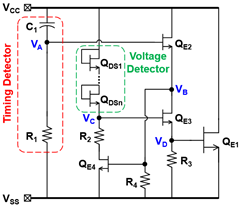
Due to the issues of standby leakage or transient leakage present in the above three references, a new design addressing these two leakage issues has also been proposed, published in an internationally renowned journal.IEEE Transactions on Electron Devices[10]. This new circuit architecture diagram is shown in Figure 13. This design utilizes a dynamic time voltage dual detection function, so this circuit will only turn on transistor Q when an electrostatic event occurs.E1In order to discharge, the circuit will not be falsely activated in the scenarios of normal power-up or rapid power-up, thus completely solving the problem of instantaneous leakage. In addition, since the voltage detector of this circuit is at the end of the series path, a transistor Q is used.E4To act as a switch, thus avoiding the circuit at VCCAfter powering on to steady state, additional standby leakage occurs.
The following explains the operation of this circuit in three scenarios. First, when the circuit is normally powered up to 6 V, VCCThe rise time of the voltage is approximately 0.1 to 1 millisecond. Due to VCCThe rise rate is lower, node VAMaintain at low potential, QE2 remains off. Therefore, node VB stays at a low potential, QE4is also in the off state. In addition, the threshold voltage (V of HEMTth) is 1.46 V. Since VCCThe voltage rating is 6 V, which is below the conduction voltage of the voltage detector. Therefore, node VC stays at a low potential, QE3Will be closed. Node VDMaintain at low potential, main discharge component QE1In the off state. Therefore, under normal power-up conditions, there will be no leakage path.
Second, under fast power-on conditions, VCCThe rise time of the voltage is approximately 10 nanoseconds. Due to VCC has a higher rise rate, node VAWill be coupled to high potential, QE2will conduct. Then, node VBRising to high potential, QE4 conducts. However, since VCCThe voltage rating is 6 V, which is below the turn-on voltage of the voltage detector. Node VCMaintain at low potential, QE3 remains off. Therefore, node DMaintain at low potential, main discharge component QE1In the off state. Therefore, no transient leakage current will occur under fast power-up conditions. After the power-up reaches a steady state of 6 V, no leakage paths will occur.
Third, when ESD strikes the VCC pin, VCCThe rise time of the voltage is approximately 10 nanoseconds. Due to VCCThe rising rate is higher, node VAWill be coupled to high potential, QE2Will conduct. Node VBRise to high potential, QE4Conduction. Due to the sufficiently high electrostatic potential, the voltage detector will conduct, node V.CWill be pulled to a higher potential to turn on QE3. Since QE2 and QE3All opened, node VDWill be charged to a high potential, the main discharge component QE1will conduct to release a large amount of ESD current.
4.3 Comparison of References
For the aforementioned literature, several important indicators have been consolidated for evaluation, as shown in Table 2. Reference [7] does not provide information on the size and layout area of the main discharge component HEMT in the article. In references [8], [9], and [10], the total channel width of the main discharge component HEMT is 6000 micrometers. In terms of HBM electrostatic tolerance, references [7], [8], [9], and [10] have HBM levels of 3000 V, 6250 V, 6000 V, and 6250 V, respectively. Regarding DC standby leakage current, reference [7] has a leakage current of 3.81 μA; reference [8] has a leakage current of 0.1 nA, which is the lowest among all designs due to the absence of a leakage path; reference [9] has a leakage current of 11 nA, which is attributed to the leakage path in its detection circuit.DSTransistor (Cascode structure). The design in reference [10] excludes the series connection of Q in the voltage detector.DSThe leakage current path caused by the transistor, thus also has a low leakage current of only 0.8 nA. Regarding the instantaneous leakage in the scenario of fast power-up, references [7], [8], [9] are mainly based on the rising time detection function realized by capacitive coupling circuits, so they cannot solve this problem. However, the design in reference [10] utilizes a series of Q.DSTransistors achieve voltage detection functionality, thus effectively solving this problem.
Table 2, Comparison of references for electrostatic discharge protection circuits between power rails.
|
Test object |
Reference [7] IEDM’23 |
Reference [8] ICMTS’24 |
Reference [9] JEDS’24 |
Reference [10] T-ED’25 |
|---|---|---|---|---|
|
Design Concept |
Improved Capacitive Coupling |
Capacitive Coupling |
Improved Capacitive Coupling |
Dynamic Time Voltage Dual Detection |
|
ESD discharge components Total channel width |
N/A |
6000 μm |
6000 μm |
6000 μm |
|
Chip area |
N/A |
201650 μm2 |
219040 μm2 |
99241 μm2 |
|
HBM electrostatic discharge tolerance |
3000 V | 6250 V | 6000 V | 6250 V |
|
Standby leakage @ 6V |
3.81 μA | 0.1 nA | 11 nA | 0.8 nA |
|
Can it prevent rapid power-on? Transient leakage generated |
No | No | No | Yes |
5. Conclusion
The development of electrostatic discharge protection technology for Gallium Nitride (GaN) chips currently has two main directions. One is the gate electrostatic discharge protection design for discrete components, and the other is the electrostatic discharge protection circuit necessary for full-chip protection between power rails. Regarding the gate electrostatic discharge protection design for discrete components, in addition to considering the ability to effectively provide a discharge path when electrostatic discharge occurs, thereby reducing the clamped gate voltage level, it is also necessary to consider whether the additional electrostatic protection circuit will affect the normal function of the original circuit or the switching speed of the GaN device, especially considering the application of negative gate voltages, which adds more challenges to the design. Regarding the design of the electrostatic discharge protection circuit between power rails, in addition to the circuit itself needing to have sufficient electrostatic protection capability, attention must also be paid to the level of clamped electrostatic voltage in the circuit. Furthermore, since the electrostatic discharge protection circuit between power rails exists between the power supply and ground, the size of the standby leakage current after the circuit reaches a steady state will directly affect the chip's power consumption. How to reduce standby leakage current is a very important issue. Additionally, rapid power-up scenarios can cause instantaneous leakage problems, and how to enable the circuit to clearly distinguish between electrostatic events and rapid power-up events to avoid malfunctions during rapid power-up is also an important design direction for saving chip power consumption.
Reference:
[1] Wide bandgap semiconductors: pursuing the promise (DOE/EE-0910), U.S. Department of Energy, Advanced Manufacturing Office. April 2013.
[2] K. J. Chen et al., "GaN-on-Si power technology: devices and applications," IEEE Trans. Electron Devices, vol. 64, no. 3, pp. 779-795, March 2017, doi: 10.1109/TED.2017.2657579.
[3] T. J. Flack, B. N. Pushpakaran, and S. B. Bayne, “GaN technology for power electronic applications: a review,” Journal of Electronic Materials, vol. 45, no. 6, pp. 2673-2682, March 2016, doi: 10.1007/s11664-016-4435-3.
[4] M.-D. Ker, "Whole-chip ESD protection design with efficient VDD-to-VSS ESD clamp circuits for submicron CMOS VLSI," IEEE Trans. Electron Devices, vol. 46, no. 1, pp. 173-183, Jan. 1999, doi: 10.1109/16.737457.
[5] C.-Y. Ke, W.-C. Wang, M.-D. Ker, C.-Y. Yang, and E. Y. Chang, "Investigation on ESD robustness of 1200-V D-Mode GaN MIS-HEMTs with HBM ESD test and TLP measurement," in Proc. IEEE International VLSI Symposium on Technology, Systems and Applications, 2023, pp. 1-2, doi: 10.1109/VLSI-TSA/VLSI-DAT57221.2023.10134426.
[6] J.-H. Lee et al., "Incorporation of a simple ESD circuit in a 650V E-Mode GaN HEMT for all-terminal ESD protection," in Proc. IEEE Int. Rel. Phys. Symp. (IRPS), 2022, pp. 2B.3-1-2B.3-6.
[7] T.-W. Wang et al., “ESD HBM 3kV discharge for monolithic GaN-on-Si HEMTs integrated chips,” in IEDM Tech. Dig., 2023, pp. 1-4, doi: 10. 1109/IEDM45741.2023.10413733.
[8] W.-C. Wang and M.-D. Ker, "Test structures to investigate ESD robustness of integrated GaN devices," in Proc. IEEE Int. Conf. Microelectronic Test Structures, 2024, pp. 1-4, doi: 10.1109/ICMTS 59902.2024.10520680.
[9] W.-C. Wang and M.-D. Ker, "Fully integrated GaN-on-Silicon power-rail ESD clamp circuit without transient leakage current during normal power-on operation," IEEE J. Electron Devices Society, vol. 12, pp. 760-769, 2024, doi: 10.1109/JEDS.2024.3462590.
[10]C.-Y. Ke and M.-D. Ker, “Design of GaN-on-Silicon power-rail ESD clamp circuit with ultralow leakage current and dynamic timing-voltage detection function,” IEEE Trans. Electron Devices, vol. 72, no. 3, pp. 1066-1074, Mar. 2025, doi: 10.1109/TED.2025.3529405.


