
High-resolution non-destructive three-dimensional morphology analysis technology and industrial applications
In recent years, with the rapid development of high-performance computing (HPC), artificial intelligence (AI), advanced packaging (2.5D / 3D IC), and high-density PCB technology, the component structure continues to shrink, and the process tolerance has significantly decreased. Surface roughness, structural height differences, microstructure profiles, and packaging morphology control have become key factors affecting yield and reliability.
In response to the demand for nanoscale morphology analysis, MA-tek has partnered with Sensofar, a company recognized in the global precision surface measurement field, to introduce the Sensofar S Neox optical three-dimensional surface morphology measurement system. This system integrates confocal microscopy, white-light interferometry, and focus variation technology to provide high-resolution, non-destructive, full-field three-dimensional measurement capabilities.
-
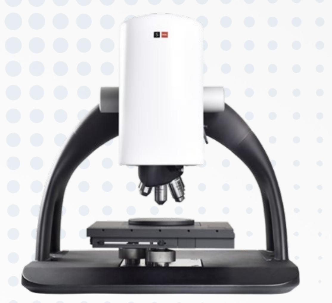 Appearance of the SENSOFAR 3D Optical Profiler
 -
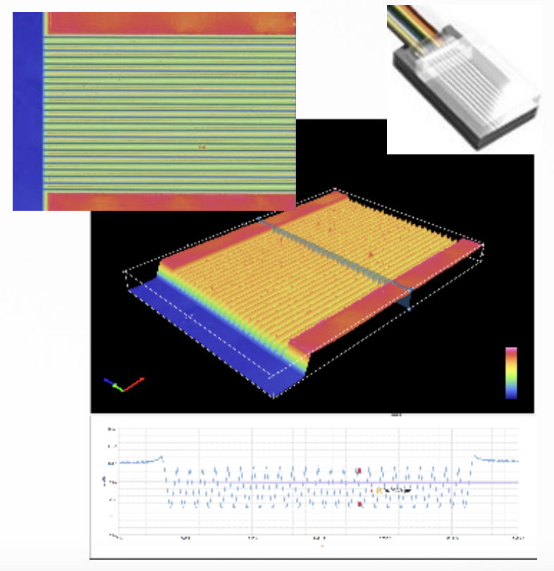 Scanning Results of a Silicon Photonic Component
Optical three-dimensional surface morphology measurement systems focus on morphology measurement, for example:
- Surface roughness (Ra / Rq / Sa / Sq)
- Microstructure height and depth analysis
- Line width / Line height / Line length measurement
- Copper Pillar and Solder Ball 3D Profile
- Silicon photonic structure morphology analysis
- Crater test depth and width measurement
- IC packaging laser marking profile analysis
In advanced packaging processes, uneven copper pillar height, abnormal plating morphology, and poor depth control of vertical vias (such as TSV and Via) may lead to stress concentration and subsequent reliability issues. Through high-resolution three-dimensional morphology reconstruction, the process status can be monitored in real-time, and key parameters can be optimized.
Technical Advantages
1. Non-contact, non-destructive measurement
To avoid probe indentation and sample contamination, suitable for brittle materials and high-value samples.
Nanometer-level high resolution
White-light mode height resolution can reach sub-nm level.
Confocal mode can measure high slope structures (up to about 72°)
3. Diverse Surface Adaptability
- Rough surface → Confocal mode
- Ultra-smooth surface → White-light mode
- Focus Variation
4. Support for large-sized samples
- The maximum measurement area can reach 2 cm × 2 cm.
- Supports 12-inch silicon wafer measurement
- Can operate in atmospheric environment.
Applicable application fields
✔ Semiconductor Process and Packaging Analysis
✔ Analysis of PCB Copper Film Roughness and Via Depth
Precision machining and microelectromechanical components
Medical implant surface quality inspection
Materials Science Nanostructure Research
MA-tek integrates advanced optical three-dimensional surface morphology measurement systems by importing confocal, white light interference, and Focus Variation technologies, providing high-resolution, non-contact, and non-destructive three-dimensional measurement capabilities. This helps customers grasp process variations in real-time, optimize key parameters, and establish a robust process foundation early in product development.
➤ Further Reading:Complete Introduction to Optical 3D Surface Topography Measurement Technology


