MA-tek News
07.12
2026
MA-tek silicon photonics analysis and testing layout completed!
As AI, high-performance computing (HPC), and Co-Packaged Optics (CPO) rapidly develop, data transmission is shifting from "electric" to "optical," and Silicon Photonics has become the core technology for semiconductor testing in the next generation of high-speed computing and optoelectronic integration.
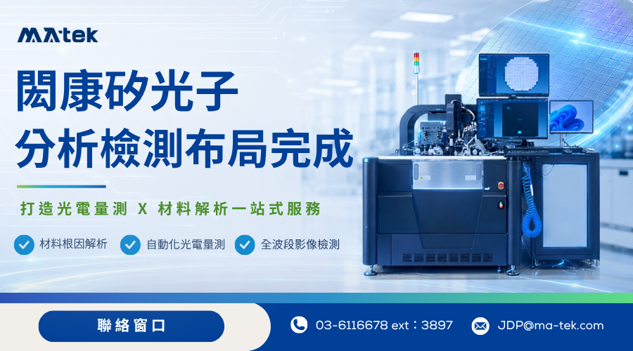
MA-tek deepens its layout in silicon photonics analysis and testing, creating a complete optoelectronic verification service platform. Currently, it has completed the establishment of the first set of internationally leading silicon photonic wafer and chip analysis verification equipment, officially providing one-stop, automated, and highly repeatable optoelectronic characteristic measurement and failure analysis services, assisting customers in accelerating component development, packaging process optimization, and product mass production verification.
 Advanced Silicon Photonics Measurement EquipmentIntegrating top-tier automated temperature-controlled probe stations with full-band near-infrared optical imaging systems, it can support various silicon photonic optoelectronic characteristic measurements and component characteristic analysis under different temperature conditions.
 Complete Optical Performance AnalysisProvides measurements of insertion loss (IL), reflection loss (RL), wavelength scanning, coupling efficiency, leakage light location, etc., to comprehensively grasp the quality of optical signal transmission and component performance.
 Passive Optical Component AnalysisSupport analysis of waveguides, grating couplers (GC), edge couplers (EC), etc., to quickly locate waveguide defects, leakage positions, and process anomalies.
 Active optoelectronic component verificationFor components such as modulators and photodetectors, complete static and dynamic optoelectronic characteristic analysis is provided to verify high-speed optoelectronic conversion performance and reliability.
 Root Cause Failure Analysis of MaterialsCombining advanced material analysis techniques such as SEM, FIB, TEM, STEM, SIMS, and SCM, we trace from optical anomalies to material defects, waveguide sidewall roughness, doping distribution, and process issues, providing a complete failure analysis solution.
From automated optoelectronic measurements, full-band near-infrared optical imaging analysis, to material microstructure and root cause analysis, MA-tek provides a complete silicon photonics analysis and testing service, welcoming new opportunities in the era of AI, CPO, and silicon photonics together with you!