Secondary Ion Mass Spectrometry (SIMS) in the Analytical Applications of Quality Monitoring in Integrated Circuit Processes
With the advancement of technology, the market demands for electronic products are increasing, requiring smaller product sizes, faster operating speeds, and more functions. This has led to the emergence of smartphones, AI servers, and cloud data centers, all of which require high-performance and compact IC chips. To enhance the speed of semiconductor chips, increase component integration density, and reduce power consumption, semiconductor components are continuously being miniaturized. The evolution of semiconductor processes has progressed from the 3μm process in the 1980s to the current 3nm FinFET (Fin Field-Effect Transistor) and nanosheet gate-all-around (GAA) transistors. As shown in Figure 1, the cutting-edge technology has officially entered the mass production technology node below 3nm.
Top semiconductor application chips not only require excellent IC circuit design but also need perfect nano-device structures combined with next-generation or advanced semiconductor process technologies to achieve optimal chip performance. Common materials in the process include Strain Si (SiGe / SiP), Gate Oxide, dielectrics, and ion implantation of boron (B), phosphorus (P), arsenic (As) to control device characteristics. The analysis techniques required for detecting these materials or components include two aspects: (1) high spatial resolution (less than 1nm) or (2) advanced analysis techniques capable of detecting low component concentrations (less than ppm). This article mainly introduces the application cases of Secondary Ion Mass Spectrometry (SIMS) in the quality control monitoring of IC processes.
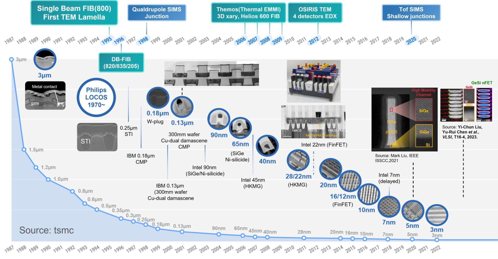
Figure 1. Evolution of semiconductor processes and application of analytical techniques
Case 1 Strained-Si
In the evolution of Si MOSFET device process miniaturization, how to increase the mobility of electrons and holes in the channel is an important issue for enhancing device performance. Among the methods to improve electron and hole mobility, strain engineering (Strained Engineering, Strained-Si) is one of the most effective ways to enhance the performance of Si nanoscale devices. In strain engineering, SiGe materials are commonly used to increase the compressive stress in the PMOS channel, thereby increasing hole mobility, while SiP materials are used to increase the tensile stress in the NMOS channel, reducing contact resistance and increasing electron mobility. Regardless of whether it is SiGe or SiP materials, slight changes in composition can significantly affect the degree of strain. Therefore, accurately detecting and analyzing the composition of SiGe and SiP, while simultaneously analyzing trace doping components, requires the use of SIMS for analysis. Figure 2 shows the SIMS depth profile analysis results of SiGe and SiP.
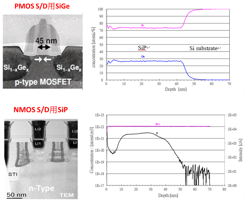
Figure 2. SIMS application in depth analysis of Strain Si (SiGe & SiP)
Case 2: High Dielectric Constant Material Gate Oxide (SiON)
The gate oxide layer in metal-oxide-semiconductor field-effect transistors (MOSFETs) is an important insulating material that controls the channel switch of the device, and it is also a critical structural material for controlling gate leakage. The higher the dielectric constant of this gate oxide layer, the better the characteristics of the entire device. In practical applications of high dielectric constant materials, different high dielectric constant materials are chosen as gate oxide layers according to the different device requirements and process nodes. Among them, Oxynitride (SiON) is a commonly used high dielectric constant material. SiON has many applications, such as gate oxide layers, diffusion barrier layers, etching stop layers, flash memory, dynamic random-access memory (DRAM), etc. The content of components such as oxygen (O) and nitrogen (N) in SiON materials for each application may vary due to different processes and requirements. Figure 3 shows a case of using SIMS to analyze the high dielectric constant material Gate Oxide (SiON).
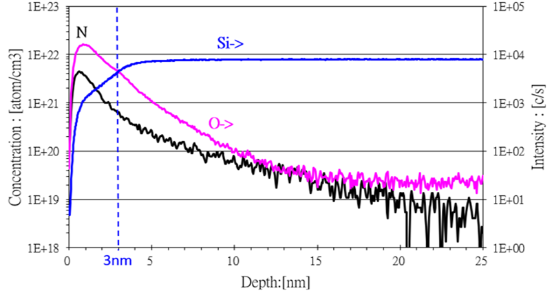
Figure 3. High dielectric constant material Gate Oxide (SiON) is commonly used in the oxide layer of semiconductor devices such as Metal-Oxide-Semiconductor Field-Effect Transistors (MOSFETs), with a thickness ranging from several tens to several nanometers.
Case 3 BPSG (Boro-phospho-silicate Glass)
In semiconductor processes, the front-end process (FEOL, Front End of Line) refers to the part of making components, while the back-end process (BEOL, Back End of Line) refers to the part of making metal wires and insulating dielectric layers. The connection between the front-end and back-end is made through conductive materials at the contact windows. The filled non-conductive dielectric material is called ILD (Inter-Layer Dielectric). The process of making contact windows and filling non-conductive dielectric materials is collectively referred to as the middle-end process (MEOL, Middle End of Line). Because the surface is uneven after the completion of the front-end process, materials with good filling capabilities are required for filling, and these materials also need to have appropriate insulating properties. Commonly used filling materials are BPSG or PSG. BPSG is silicon glass with added elements such as B (boron) and P (phosphorus). The content and ratio of B and P will affect the flowability and filling capability of the material, and will also influence the parameters of subsequent etching processes. Therefore, understanding the content, distribution, and composition ratio of B and P is an important parameter that needs to be known when using this material in the process. Figure 4 shows the SIMS analysis results of BPSG (Boro-phospho-silicate Glass).
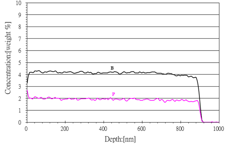
Figure 4. SIMS analysis results of BPSG (Boro-phospho-silicate Glass)
Case 4 FSG (Fluorinated Silicon Glass)
The previously mentioned back-end-of-line (BEOL) process refers to the part of the manufacturing that involves creating metal interconnects and insulating dielectric layer materials. The actual process requirements dictate that the metal interconnects need to be made from low-resistance materials, while the insulating dielectric layer materials need to be low-k (low dielectric constant) materials. These two types of materials are used to reduce the overall RC (resistance-capacitance) delay of the IC. Low dielectric constant materials are typically achieved by incorporating elements such as carbon (C) or fluorine (F) into silicon dioxide to lower the dielectric constant. Therefore, the amount of C or F added is a crucial factor affecting the dielectric constant of the material. FSG (Fluorinated Silicate Glass) is one of the commonly used low-k materials, which is created by adding fluorine (F) to silicon dioxide to reduce the dielectric constant of the material. Figure 5 is an example of using SIMS to accurately determine the fluorine content in FSG.
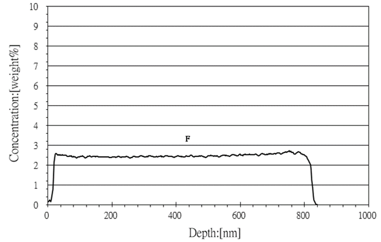
Figure 5. SIMS depth profile analysis results of FSG
Case 5: New type of ternary functional film material SiCN
The new ternary functional film material SiCN has many advantages such as high hardness, wide optical bandgap, good high-temperature oxidation resistance, and corrosion resistance, making it applicable to products like ICs, LCDs (liquid crystal displays), FPDs (flat panel displays), and optoelectronic components. The ratio and uniformity of C/N in this material significantly affect its properties. Figure 6 shows a SIMS analysis case of SiCN.
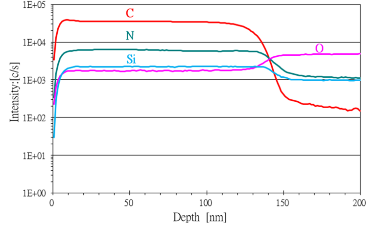
Figure 6. SIMS depth profile analysis results of SiCN
Case 6 Diffusion Analysis (Backside SIMS)
The analysis method of Backside SIMS can improve the knock-in effect of the elements being tested from high concentration layers to low concentration layers. This is particularly helpful for studying the downward diffusion analysis of metal layers. Using the general surface analysis method, a small amount of metal can easily be pushed into the lower layers during the analysis process, creating a false impression. The Backside SIMS analysis technique can avoid this problem and obtain the true vertical distribution of metal composition. Before Backside SIMS analysis, the substrate needs to be thinned to achieve a flat surface, requiring good sample preparation techniques. Figure 7 shows the results of studying copper diffusion through general front analysis and backside analysis.
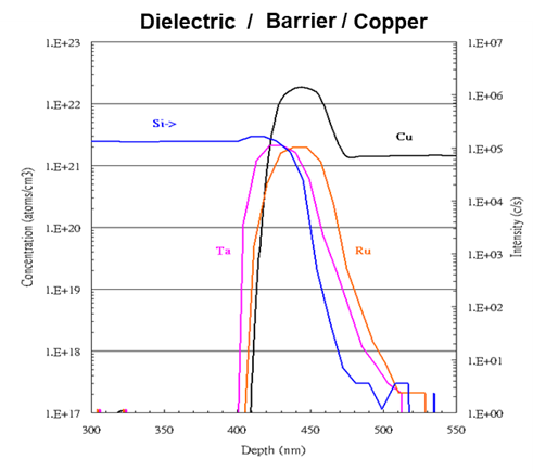
Figure 7-1. During the analysis of surface SIMS, copper is pushed into the lower layers due to the gradual bombardment of the SIMS ion beam during the analysis process.
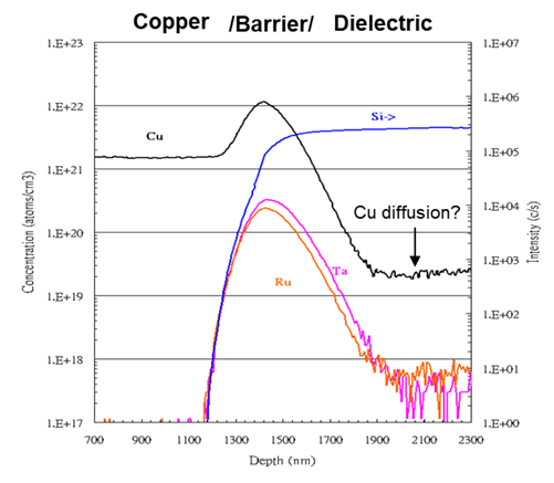
Figure 7-2. Backside SIMS analysis can truly present the distribution of copper diffusion and has good depth resolution.
Case 7 Organic Contaminant Analysis
Generally, FT-IR is prioritized for organic matter analysis. When organic pollutants are present in the surface layer, FT-IR may not be able to detect them due to insufficient signal strength. Time-of-Flight Secondary Ion Mass Spectrometry (TOF-SIMS) can analyze the mass spectrum to compare normal products with abnormal products (or suspected pollutants), and determine possible organic pollution sources through mass spectrum comparison. Figure 8 shows a TOF-SIMS analysis case of organic contamination, where the mass spectrum comparison identified contamination from silicone oil during the packaging process, resulting in the epoxy not adhering properly to the chip.
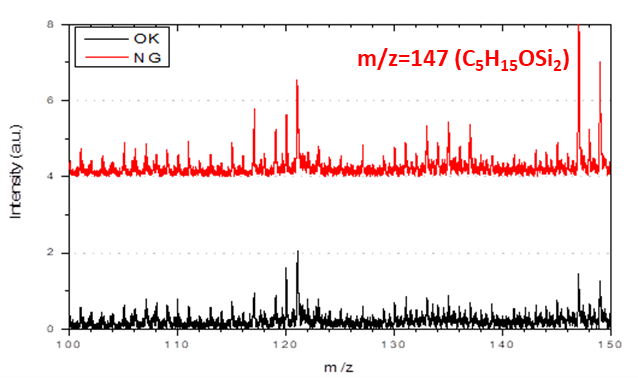
Figure 8-1. The presence of organic contaminants during the packaging process causes the epoxy to fail to adhere properly to the chip.
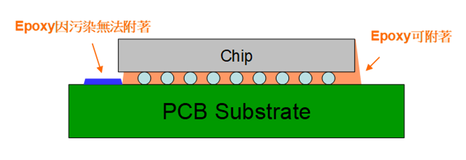
Figure 8-2. Analysis comparison via TOF-SIMS surface mass spectrometry to determine the contaminant as silicone oil.
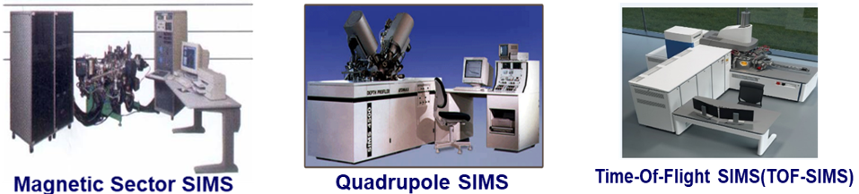
Secondary Ion Mass Spectroscopy (SIMS) analysis involves bombarding a sample with an energetic ion beam to excite secondary ions. The secondary ions are accelerated into a mass spectrometry analysis system, where they are separated based on their mass-to-charge ratio (m/e) using electric and magnetic field deflections, achieving the goal of compositional analysis. The intensity of the secondary ions can be converted to obtain the concentration of elements, while the ion bombardment time can be converted to depth distribution. SIMS has an excellent detection limit, capable of measuring element concentrations in solid materials down to parts per million or below (ppm-ppb). SIMS is divided into three types: Magnetic-Sector SIMS, Quadrupole-SIMS, and TOF-SIMS; Magnetic-Sector SIMS has the best detection limit, suitable for micro-pollution analysis; Quadrupole-SIMS has good depth resolution, suitable for thin film and ultra-shallow junction analysis; TOF-SIMS, in addition to organic analysis, has the latest models with depth analysis capabilities comparable to those of Quadrupole-SIMS. Table 1 compares the characteristics of the three types of SIMS.
MA-tek has a complete range of SIMS models and rich practical experience, providing customers with comprehensive surface analysis services.
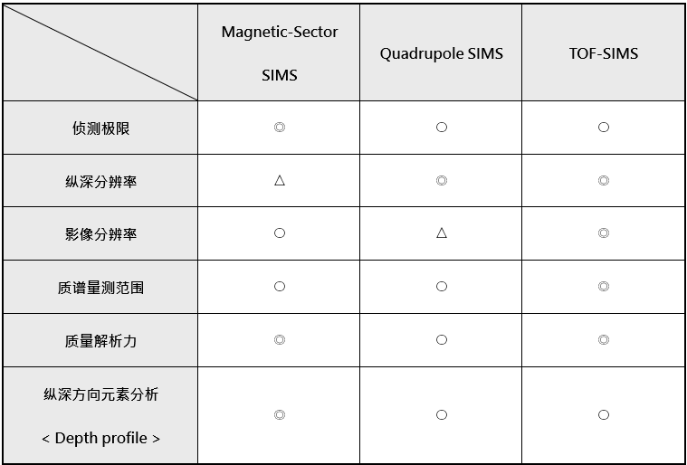
Table 1. Comparison of the characteristics of three types of SIMS