
Breaking the Limits of Moore's Law: Key Applications of Advanced Packaging Technology and Heterogeneous Integration Analysis
Moore's Law predicts that the number of transistors on an integrated circuit will double every 18 months on the same area, and the performance of chips will continue to improve. After leading the semiconductor industry for nearly 60 years, this law is gradually approaching its limits. Major manufacturers are also exploring new solutions to continuously enhance the overall performance of chips without being able to shrink transistors. They aim to achieve performance breakthroughs by stacking semiconductor circuits through system integration, with the key technology lying in the "heterogeneous integration" solutions of packaging to extend Moore's Law. The greatest advantage of advanced packaging is that it significantly shortens the distance of metal interconnects between different bare chips, thus greatly improving transmission speed and reducing power loss during the transmission process.
Currently, various wafer fabs and packaging factories are developing their own advanced packaging technologies. In terms of technology and capital expenditure, Intel and TSMC are the most proactive, with the combined capital expenditure of the two accounting for 55% of the entire industry, and their technology is also the most advanced.
__25K13ZZPQS.png "01 (4)")
Figure 1 Investment amounts and shares of various international manufacturers in advanced packaging [1]
In the case of TSMC, its advanced packaging technology can be divided into 2D InFO (Fan-Out Packaging), 2.5D CoWoS (Chip on Wafer on Substrate), and 3D SoIC. Among them, InFO technology is the most mature and the cheapest, accounting for about 70-80% of its advanced packaging capacity (80,000 to 100,000 pieces per year), and has been widely used in Apple's A-series and M-series chips. In recent years, the demand trend for AI chips has been enormous, further driving the capacity demand for advanced packaging CoWoS, which has also brought a new look to the semiconductor industry's often overlooked "testing" sector due to the advanced packaging boom. MA-tek has also continued to maintain a strategy that keeps pace with industry trends, possessing very rich analytical experience in failure analysis for advanced packaging. Below, we will decode its key application tools and technologies one by one.
__25K13jZmve.png "02 (3)")
Table 1: TSMC's 3D Fabric platform has a complete layout and is adopted by important customers.
2D X-ray
X-rays generated by high-energy impacts on metal targets have penetrating properties, allowing imaging to observe and determine whether phenomena such as cold solder joints, HIP, or Hop exist inside advanced packaging. This tool can also quickly confirm whether there are defects such as broken wires and severe melting inside the package.
__25K13xQBVd.png "03 (4)")
Figure 2: 2D x-ray is like a health check for packaging, responsible for inspecting the internal structure of the package and checking for defects.
SAT ultrasonic scanning microscope
SAT, also known as CSAM, forms images based on the different reflection rates and return energies of ultrasonic waves on materials of varying densities. Different frequency probes are selected according to the penetration rate of the ultrasonic waves to detect abnormalities such as delamination, voids, or cracks at various interface layers within advanced packaging.
__25K13KYOEP.png "04 (3)")
Figure 3 SAT plays a role in querying internal defects in packaging inspection.
3D x-ray
Under what circumstances is it necessary to use a 3D X-RAY machine? When there is only one failed sample and destructive analysis cannot be performed directly, we recommend executing ultra-high resolution non-destructive 3D X-RAY on the abnormal area. MA-tek currently has ZEISS Xradia 520 and 620 Versa high-resolution 3D X-ray Microscope devices. The principle is to bombard a metal target (W) with high-energy electrons, generating short-wavelength, high-energy, and highly penetrating X-ray radiation that penetrates the test object to produce diffraction waves. The detector receives these waves, which are converted into visible images through a scintillator, and by rotating the sample 360 degrees on the stage, various 2D X-ray tomographic images from different orientations in space are obtained. These images are then combined into a 3D X-ray tomographic image of the test object using computer calculations, which is also the principle of computed tomography imaging. The resolution of 3D X-ray depends on pixel size; the smaller the pixel size, the better the resolution. Currently, the machine's spatial resolution limit is 0.5um, and there are 12 standard filters that can be automatically adjusted within the machine, with 5 types of lenses (0.4X, 4X, 20X, and 40X) available for use.
__25K13oDrrq.png "05 (3)") Figure 4 Hardware architecture of 3D X-ray
Figure 4 Hardware architecture of 3D X-ray
The advanced packaging structure is relatively complex. If the failed samples can narrow down the abnormal range through electrical analysis, 3D X-Ray can identify obvious defects at a better scanning resolution. The following is mainly an example of scanning CoWoS samples. In Figure 5(a), the abnormal displacement of TSV can be clearly seen. In Figure 5(b), there is a delamination phenomenon in the dielectric layer (Interposer). In Figure 5(c), there is a significant anomaly at the u-bump junction.
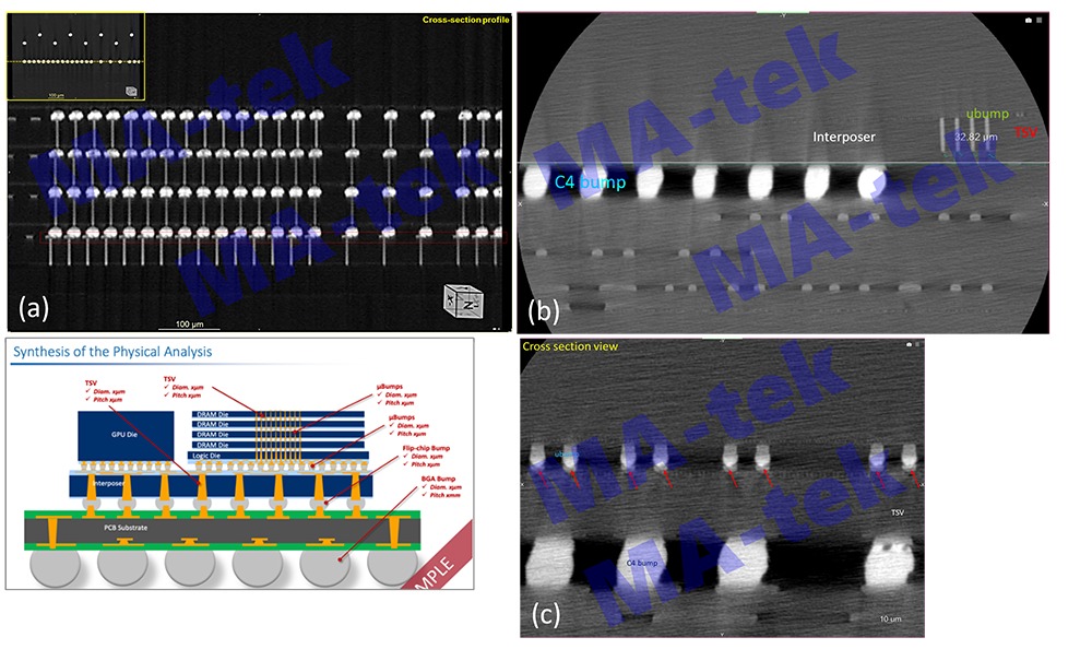
Figure 5 CoWoS packaging structure diagram[3] and common defect types
TDR Time Domain Reflectometer
Time Domain Reflectometry (TDR) is a commonly used network analysis technique, primarily used to measure the reflection and attenuation of signals in transmission lines or transmission media. In advanced processes, TDR technology plays an important role in failure analysis, especially in quickly and conveniently distinguishing whether anomalies occur at the chip or packaging end in advanced packaging failure exclusion. It is mainly applied in semiconductor manufacturing and testing processes, as well as in the maintenance and failure exclusion of electronic devices.
TDR technology can quickly and accurately detect open circuits. Its principle is to use emitted short pulse signals transmitted along the tested circuit, such as the connections inside the package or chip, and then measure the time and intensity of the reflected signals. When the transmission line is intact, the reflected signal measured by TDR will show a typical waveform. However, if an open circuit occurs in the transmission line, the reflected signal will show abnormalities, such as a sudden decrease in the intensity of the reflected signal or its disappearance, or the time delay of the reflected signal not meeting expectations. Through the analysis results of good products, bad products, and empty boards, the location of the open circuit can be accurately determined, whether it is an open circuit in the chip within the package or in the package itself. It can even infer which structure in the package has abnormalities, such as the most common u-bump, TSV, or C4 bump structures or interface issues in advanced packaging.
__25K13Eozpn.png "07 (2)")
Figure 6 compares the TDR waveforms of good products, bad products, and empty boards, determining that the possible breakpoint is at the u-bump.
Lock-in Thermography(LIT)
LIT, also known as thermal emission microscopy, can very effectively and quickly locate failure hotspots in 2.5D and 3D advanced packaging. In addition, defective semiconductor devices often exhibit localized power variations, leading to increased localized temperatures. LIT can detect the temperature distribution on the surface of objects through infrared thermal imaging technology, thereby identifying potential faults or issues. It also utilizes lock-in infrared thermal imaging to improve the accuracy of localization, providing subsequent non-destructive (3D X-ray) and destructive slicing observations of packaging defects.
LIT uses a high-sensitivity InSb (Indium Antimonide) detector to detect the thermal radiation generated by the defect location of the object under test in an energized state, in order to locate the failure position and even estimate the relative depth distance of the heat source. Its characteristics and application overview are as follows:
- High-resolution infrared thermal imaging: Equipped with high-resolution infrared thermal imaging technology, it can capture the details of slight temperature variations on the surface of objects.
- Fault detection and analysis: By detecting abnormal temperatures on the surface of objects, potential issues can be quickly identified, such as overheating of electronic components or thermal failure of devices, etc.
- Detectable failure mechanisms: applied to product short circuits, ESD defects, oxide breakdown, device latch-up, defective transistors and diodes.
In general, thermal emission microscopy is a powerful thermal imaging analysis instrument that can assist in quickly and accurately locating faults.
__25K13eUcFY.png "08 (2)")
Figure 7thermal emission microscopyIt is possible to detect the location of the failure point on the plane without opening the cover, and it can also determine which layer of the chip or substrate the failure point exists in vertically.
Plasma FIB (P-FIB)
In the failure analysis of packaging and chips, the initial analysis method was mainly grinding and slicing. With the advancement and diversification of packaging types, the I/O density within chips has also rapidly increased. Among them, enhancing the density of interconnection points in chips is the development trend of 2.5D/3D packaging. When the gap between points is reduced to below 10 microns, manual grinding will no longer be sufficient to accurately prepare targeted sample slices, and P-FIB has gradually become one of the main techniques used in failure analysis of advanced packaging.
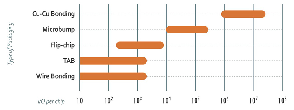
Figure 8 The number of connection points that various packaging technologies can achieve in a 1x1cm^2 chip [4]
The application of P-FIB, in addition to basic structural observation, can also be used for detection and verification after hotspot or non-destructive analysis. For example, after observing anomalies with Thermal Emission Microscopy, OM, 3D X-ray, or SAT, P-FIB can be utilized to confirm the cross-section at the anomaly.
__25K13s2suA.png "10 (1)")
Figure 9 (a) Observing the TSV deformation position using 3D X-ray and (b) performing P-FIB rough milling + FIB fine milling.
DB P-FIB cutting area can reach 500um wide and 500um deep, which can be used to observe the structure of advanced packaging, such as C4 bump/interposer/u-bump/TSV/fine pitch RDL. During the cutting cross-section process, the cutting situation can be observed in real-time using SEM, allowing for immediate assessment of defect changes.
__25K13TRHz7.png "11 (1)")
Figure 10 Continuous process of FIB cutting TSV
Sample preparationP-Lapping
Sample preparation plays a crucial role in failure analysis and is the biggest factor determining the success rate of the analysis, especially in the advanced packaging failure analysis process. Through the preparation process, including manual/automatic grinding, chemical etching, and other steps, every detail tests the experience and attentiveness of the operators. The MA-tek team has rich experience in the high-end advanced packaging field, and with mature sample preparation capabilities, we have successfully discovered various defects inside the packaging.
-
__25K13DSsgz.png)
Figure 11 P-Lapping Manual Grinding Technology (BGA)
-
__25K13cHKAL.png)
Figure 12 P-Lapping manual grinding technology (InFO_oS) [7]
SEMSample preparation pre-treatment
Sample preparation and pre-treatment, along with observation using electron microscopy, are commonly used methods for failure analysis in advanced packaging. The processing methods directly affect the final observation and analysis results. Below are several important properties of SEM sample preparation.
- Removal of Contaminants and Impurities: SEM can observe the surface of samples with extremely high resolution, so before observation, the samples must be properly cleaned to remove any impurities that may affect the results or any liquids, volatiles, and dust that may contaminate the machine.
- Improve conductivity: SEM samples require good conductivity to avoid electrostatic discharge during the analysis process, which can damage the samples and interfere with image capture. Therefore, some non-conductive materials are coated with gold or carbon before SEM imaging to improve image quality.
- Proper fixation and cutting: Due to the limited size of the SEM stage, samples need to be cut to facilitate fixation on the stage. Currently, the model used by MA-tek can accommodate samples up to six-inch wafers in size, with a height limit of 1.5 centimeters. Commonly used materials can be cut, such as wafers, substrates, ceramic materials, metals, glass, and polymer materials.
- Obtaining information from specific areas: If there are specific vertical structures that need to be observed, point sample preparation (sectioning) is required. Through grinding and polishing, and even ion beam sectioning, we can precisely cut structures to about 1um in size for SEM imaging. Smaller targets can also be prepared and imaged using FIB and TEM.
- Improving resolution and contrast: Proper sample preparation can help enhance the resolution and contrast of SEM. We obtain more sample information through some surface treatments, commonly used methods include chemical surface etching, ion beam surface polishing or deep cutting, plasma cleaning, etc.
Through the related methods introduced above, we must first embed the samples in epoxy resin before grinding. The purpose is to protect the structure of the samples and avoid damage to the sample layers during the grinding process. At the same time, we must pay attention to the grit size and materials of the sandpaper used, to avoid unnecessary damage to the samples caused by overly large sandpaper particles. Finally, we use polishing liquid and velvet cloth for the final processing, so as to obtain a smooth and flat cross-section, facilitating SEM imaging and abnormal observation.
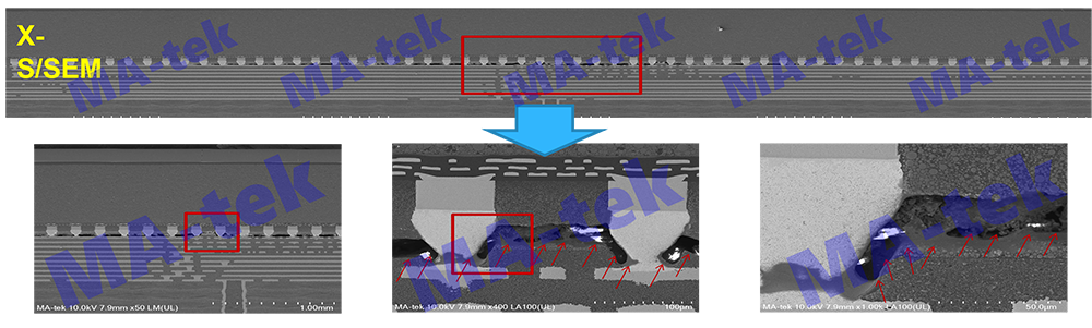
Figure 13 BGA packaging is polished and then observed under SEM for abnormal areas.
Riding the wave of AI, the output value of high-performance chips and advanced packaging is increasingly growing in the semiconductor industry. The complexity in design and structure poses unprecedented challenges for failure analysis. In the failure analysis of advanced packaging, adhering to the various aspects and essence described in this article will certainly be of great help in defect localization and observation.
Reference:
[1] Yole
[2] Fugle
[3] EETimes
[4] King-Ning Tu, Chih Chen, Hung-Ming Chen, Electronic Packaging Science and Engineering, Wiley, 2021
[5]https://www.matek.com/zh-TW/Tech_Article/detail/specialist-column/all/202207-IAR (3D IC Packaging: Ultra High Density Copper-Copper Heterogeneous Bonding)
[6] https://www.matek.com/zh-TW/services/index/P-FIB
[7] https://3dfabric.tsmc.com/chinese/dedicatedFoundry/technology/InFO.htm


