
The new battlefield of two-dimensional semiconductors: bismuth selenide transistors
The new battlefield of 2D semiconductors:bismuth selenide transistors
Yang Yueh-Chiang, Chiu Po-Wen
-
tracing back to the source
Transistors continue to improve the performance of silicon-based integrated circuits (ICs) under the impetus of Moore's Law. As the scale shrinks below the 10 nanometer technology node, it is approaching the physical limits of the components in operation. Despite design technology co-optimization (DTCO) and FinFET technology shrinking the scale to the 5 nanometer technology node, controlling short-channel effects remains the most severe challenge for silicon-based transistors. Therefore, transistors with channels made of two-dimensional materials at atomic thickness below 1 nanometer have become a research hotspot. The diverse atomic stacking structures of two-dimensional materials endow many novel physical phenomena and outstanding device performance: ultra-high carrier mobility, low-loss dielectrics, superconductors under Moore's lattice, tunable metal-semiconductor contacts, ballistic transport under surface doping, ferromagnetic order under heterostructures, and valley polarization effects, making them candidates for post-silicon era devices. At the same time, silicon-based integrated circuits are facing extremely complex integration programs and device compatibility issues with new types of field-effect transistors (FeFET, TFET, DSFET, SFET, FFET), which must confront new challenges beyond the Von Neumann architecture. Looking ahead, the arrival of the scaling limits of complementary metal-oxide-semiconductor (CMOS) technology requires more special structural designs (VGAA, VTFET) or next-generation materials to replace silicon-based ones to meet the standards for the continuation of Moore's Law. Here, we will introduce the novel two-dimensional material - bismuth selenide semiconductor, and its excellent device characteristics, which are expected to become a new observer on the International Roadmap for Devices and Systems (IRDS).
In the mid-20th century, breakthroughs in point-contact transistors at Bell Labs, along with the emergence of junction transistors, aimed to allow electrons bound by surface states in semiconductors to achieve current amplification and rectification within transistors through field effects. However, germanium was introduced earlier for radar detectors, making germanium transistors the subject of earlier research. Over time, scientists discovered that germanium could not be effectively operated in higher electric fields due to its low melting point limitations. Meanwhile, silicon, a member of the same group, exhibited higher thermal stability, gradually shifting focus to research on silicon wafers. Additionally, the successful doping of boron and arsenic into silicon wafers using the "high-temperature gas diffusion method" formed P-type and N-type regions in semiconductors. The use of the "thermal oxidation method" to control the growth of silicon dioxide thin films not only reduced the impact of surface states in silicon semiconductors but also allowed the native oxide layer to serve as a high-quality insulating interface. Consequently, the subsequent extensive research on silicon-based semiconductors led to the advent of "metal-oxide-semiconductor field-effect transistors" (MOSFETs), providing a rich foundation for integrated circuits in the 21st century.
The development of the integrated circuit industry has evolved from the era of manually soldering connections between discrete components to incorporating resistors, capacitors, and transistors into silicon-based integrated circuits. The planar transistors can be seen as the basic units of integrated electronics. With the increasing demand for high-speed computing and storage capacity, the density and complexity of chips have also been growing day by day. It is worth mentioning that before the 22-nanometer technology node, the advancing lithography technology allowed for a reduction in size by about 0.7 times, which resulted in proportionally reduced energy consumption and exponentially increased performance, marking the golden age driven by Moore's Law. However, this good fortune did not last long. As the component scale continued to shrink to less than 20 nanometers, the internal electric fields of the gate, source, and drain began to interfere with each other, and the wave-like properties of electrons started to dominate particle behavior. The impact of quantum effects had to be considered, and non-ideal effects at small sizes also emerged (such as threshold voltage short-channel effects (SCE) and drain-induced barrier lowering (DIBL)).
Taking Apple's A16 processor from 2022 as an example, compared to the 4044 microprocessor from the 1970s, the number of transistors has increased by about 7 million times. This shows that the two important indicators for transistor design are based on the low leakage current Gate and Source-to-Drain Leakage and the switching response Subthreshold Swing, aiming to escape the predicament of insufficient area occupied by planar structures. As early as 1999(20~22)Published by Chenming Hu's team in IEEE: "Sub 50-nm FinFET: PMOS" The initial prototype of FinFET semiconductor has already indicated that after the transition from 2D MOSFET to 3D FinFETs, the feature size can be further reduced while maintaining the gate's three-dimensional structure for channel control. In view of this, in 2016(23)Based on FinFETs, the team led by N. Loubet has constructed a vertically stacked three-layer "Gate-All-Around Field-Effect Transistors (GAAFETs)." To this day, TSMC still uses the more mature FinFET structure at the 3-nanometer node. However, below the 2-nanometer technology node, future advancements will rely on the maturity of "stacked three-dimensional integrated circuit (3DIC)" technology to continue extending Moore's Law in the vertical stacking direction. Thus, the so-called tall buildings rise from the ground, as the era of skyscraper competition will come to an end.
Looking at the technological evolution of the silicon microelectronics era, the most advanced FinFET structures still face severe challenges under miniaturization. Reducing the width of the fins means that surface roughness and dangling bonds will cause strong carrier scattering.(24)leading to a significant decrease in mobility; at the same time, it is accompanied by other non-ideal effects (velocity saturation, significant increase in leakage current and energy dissipation). Additionally, due to the inherent thickness of bulk silicon, the level of doping often only allows for single-sided gate control of the channel surface, greatly limiting the area utilization efficiency of silicon transistors. To address the above bottlenecks, the current International Technology Roadmap for Semiconductors (ITRS) assesses the next-generation requirements of complementary metal-oxide-semiconductor technology, urgently needing novel materials.(25)to replace silicon at the atomic scale limitations.
In 2004, Andre Geim and Konstantin Novoselov successfully prepared graphene using the mechanical exfoliation method.(4)and discover the special quantum physical properties of graphene (such as extremely high electron mobility, quantum conductivity phenomena, excellent thermal conductivity, high mechanical strength, zero bandgap characteristics, etc.)(26~28)2D materials with atomic-level thickness have also begun to attract significant interest from researchers. In recent years, many different types of 2D structures have been discovered, such as graphene and phosphorene, which are composed of a single element.(29)silicene(30)Geene(31)borophene(32)Hexagonal boron nitride - insulator(33、34)Metal chalcogenides - Indium selenide(5、35)Wait. Many two-dimensional materials initially also existed in bulk form, but with the continuous advancement of chemical synthesis techniques, the scientific community has gradually demonstrated the potential methods and techniques for manipulating materials at the atomic level.(36)Looking back, especially at "transition metal dichalcogenides (TMD)"(37~41)TMD has become a focus of in-depth research, possessing rich electronic properties (ranging from metallic to semiconductor), including tunable bandgap, thickness, strain, defects, doping, no dangling bonds, large specific surface area, single atomic layer thickness (about 0.6nm), and weak van der Waals forces stacking attraction between layers. It also exhibits excellent electronic and optoelectronic properties, quickly being designed by scientists for applications in various novel logic and storage devices.(42~43)。
Unlike silicon transistors, the dependence of the field effect mobility of two-dimensional semiconductors on thickness is relatively small, with a single atomic layer representing the ultimate scaling limit of thickness. Currently, molybdenum disulfide has been widely studied as a channel material for transistors, with its high field effect mobility, high current on/off ratio, low leakage current, and smaller subthreshold swing, making it a top choice after the mainstream generation of silicon. It is worth noting that the stacking combination of two-dimensional heterostructures benefits from this.(46~48)and mature large-area transfer technology(49)2D high-density array structure with silicon as the substrate(50)There are already preliminary results.(51~55)in fields such as optoelectronic logic devices, neuromorphic computing, data storage, sensors, and communication encryption.
However, 2D material transistors also face many limitations.(56、57)Materials typically need to be transferred, and during the transfer process, they may become contaminated due to polymer residues or develop defects due to stress. For example, during the high-temperature chemical vapor deposition (CVD) growth process, defects may form due to thermal desorption dissociation of atoms, or non-ideal doping issues may arise. Additionally, the inherent properties of the materials themselves also pose challenges, such as graphene lacking bandgap tunability due to its zero bandgap characteristic; hexagonal boron nitride inevitably exhibits electron tunneling phenomena at low layer counts when used as an interface dielectric.(59)Indium selenide with high electron mobility easily adsorbs water and oxygen molecules in atmospheric environments.(60)Wait. These problems often need to be overcome through precise packaging technology or heterogeneous junction design, and controlling the defect density of thin films remains a significant challenge. As of now, the synthesis of two-dimensional material films has been able to meet the demand for wafer-scale area. In most cases, the quality of material synthesis is closely related to the lattice matching of the substrate.(61)However, atomic-level defects in two-dimensional lattices(62)and the disorder of the internal and external(63)Factors such as strain, surface roughness, and charged impurities can affect the electronic properties of two-dimensional transistors.(64~66)These issues may lead to higher contact resistance, noticeable current hysteresis, significant leakage current, and scattering traps caused by surface defects and interfaces.
The current development of two-dimensional materials is unlikely to replace the mainstream role of silicon/silicon dioxide in integrated circuits in the short term.(67)Among them, the most critical factor is the integration capability of integrated circuits. First: 2D materials TMD lack high-quality native oxide layers and need to rely on atomic layer deposition (ALD) and transfer-stacked insulating layers to form gate dielectrics; second: 2D materials are prone to defects and lack precise and controllable doping methods.(68)(Substitution, defects, adsorption, intercalation doping), cannot effectively fill the trap states caused by defects, nor can it reverse carrier transport behavior (N-type and P-type) through high concentration doping; third: the large-area growth of 2D materials makes it difficult to precisely control the number of synthesized layers, which is challenging for the next generation of stacked three-dimensional integrated circuits (3DIC).(69)It requires a cumbersome and contamination-prone material transfer method for stacking; fourth, silicon semiconductor process technology is relatively difficult to be compatible with two-dimensional materials, such as interface strain and charge doping, non-selective etching systems, etc., which will reduce the overall integration of two-dimensional material systems.
Recently, foreign research teams have used bismuth trioxide (Bi2Se3Based on topological system materials, synthesized according to the Bi-Se-O phase diagram guidelines.(70~72),discovering novel bismuth selenide (Bi2O2Se) layered material system(73)(Figure 1). Bi2O2Se transistors have ultra-high carrier mobility.(74)(at low temperature >105cm2/V⋅s, room temperature can also reach >1000 cm2(V⋅s), excellent current switch ratio (on/off Ratio > 10)7), very low in-plane effective mass (m*= 0.14 ± 0.02 m0), approaching the ideal subthreshold swing (∼65 mV dec–1), and moderate bandgap (0.8eV) and environmental stability. Due to Bi2O2Se intrinsic structure and special physical properties(75~77)(self-suspended track interaction, ferroelectric phase transition, ultrafast optical carrier dynamics, quantum oscillation, changes in carrier concentration caused by selenium vacancies), as well as tunable bandgap and broad-spectrum light absorption characteristics, making it an excellent candidate material for electronics, optoelectronics, and thermoelectrics.(78~80)。
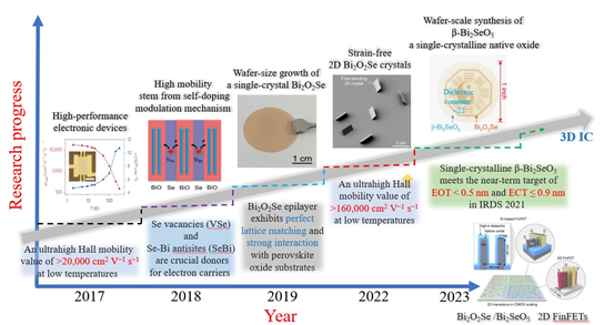
Figure 1. Bismuth selenide (Bi2O2The research program of Se) .
Bi2O2The biggest advantage of Se compared to other two-dimensional materials is its compatibility with the integration of the silicon industry.(16)。Bi2O2Se transistors can operate in room temperature environments while requiring a lower operating voltage compared to silicon (0.08 eV VS 1.12 eV); as well as wafer-scale large-area Bi2O2Se thin film growth(81、82),not only can it be through special methods (PLD(83)ALD(84)Effectively control the number of layers, while also possessing different dimensional growth orientations.(85、86)(depending on the substrate crystal plane). The biggest concern is none other than Bi2O2High-quality native oxide layer of Se Bi2SeO5has been confirmed as a good gate dielectric layer(87~89)and has selective etching characteristics(90)to meet the demand for patterned circuit design, it can be compatible with the existing silicon semiconductor industry's lithography process. Published this year in the journal Nature.(16)Using 2D Bi2O2High-quality native oxide layer of Se materials for the epitaxy of 2D FinFET array structures, with performance (high drive current and low power consumption) comparable to silicon-based FinFETs (Si-FinFET), and meeting the low power requirements of the International Roadmap for Devices and Systems (IRDS).
Seeing the small and knowing the significant
Bi2O2Se is a semiconductor formed by stacking positive and negative charge layers, due to its unique two-dimensional material structural characteristics.(74)In controlling the thickness and area of material growth, it is easier to achieve the design component requirements. In addition, the positive charge layer (Bi2O22+) is the main carrier transport channel, relative to the negative charge layer (Se that provides the carriers.2-), the scattering factors of carriers due to non-covalent bonds are effectively suppressed.(77)This enables bismuth selenide-based field effect transistors to have higher carrier mobility and transport characteristics.
Bi2O2Se was first synthesized into bulk crystals by H-Boller in 1973 using a vacuum quartz tube through solid-state reaction.(91)The team led by H. Oppermann focused on completing the quantitative work of the thermodynamic equilibrium phase diagram of the three elements Bi-Se-O in 1999. In the past decade, the synthesis methods transitioning from bulk materials to low-dimensional systems (solution or gas phase) have become increasingly mature, particularly in the chemical vapor deposition techniques for nano carbon tubes and large-area graphene.(92)Under the research foundation, two-dimensional transition metal chalcogenides have been extensively expanded and developed, and more and more controllable synthesis methods have emerged, such as: heterojunction one-step synthesis, array junction filling. Based on this foundation, we first start from Bi2Se3The study of topological properties serves as a starting point, based on Bi2Se3-Bi2O3The change of binary balanced lines, successfully prepared Bi using chemical vapor deposition.2O2Se atomic-level thin materials (<20nm). However, Bi2Se3 and Bi2O3Powder as a co-evaporation source involves a complex process, where by-products contamination and defect control are unavoidable during the decomposition and synthesis processes. It cannot effectively serve as a junction for metal semiconductors, leading to a higher residual carrier concentration. Therefore, it is necessary to reasonably select reactant species (Bi2Se3-O2、Bi2O3-Se2 as well as Bi2O2Se block material(93)) and bidirectional flow field(94)Methods to eliminate side reactions and active atomic vacancies.
Unlike the traditional van der Waals (vdWs) gap stacking of two-dimensional materials, Bi2O2Se belongs to a material characterized by the alternating stacking of charge compensation (cations and anions), with weak electrostatic interactions between layers, endowing this system with diverse electronic properties (superconductors, semiconductors, insulator characteristics). However, due to the lack of high-quality and large-area chemical vapor deposition methods for film growth, the exploration of low-dimensional materials has not become widespread. In order to understand Bi2O2The mechanism of large-area growth must first be interpreted through precise material analysis instruments (HRTEM, XRD) and imaging information to analyze Bi.2O2The precise structure of Se; as shown in Figure 2 SAED, Bi2O2Se exhibits a layered crystal structure of a tetragonal lattice (I4/mmm space group), where [Bi2O2]n2n+Covalently bonded, trapped in [Se]n2n-Inside, through weak electrostatic interactions (positive and negative charge layers), alternating stacking between layers is generated, presenting a quasi-two-dimensional structure. However, Bi2O2The strong in-plane forces of Se lead to a higher surface energy trend, tending to grow vertically into clusters.(95)To solve the problem of surface energy, a smarter approach is to use atomically flat substrates to generate stronger surface energy.(96)Mismatch dislocations with smaller lattice(97)to cause passivation or charge neutralization with high surface energy. So far, the more commonly used substrate is the surface-modified fluorinated mica (KMg3(AlSi3O10)F2), as well as the high degree of in-plane lattice matching (0.5%) and the out-of-plane lattice step epitaxial relaxation phenomenon.(81)Strontium Titanate (SrTiO)3), both of which contribute to Bi2O2Se expansion of the planar growth.
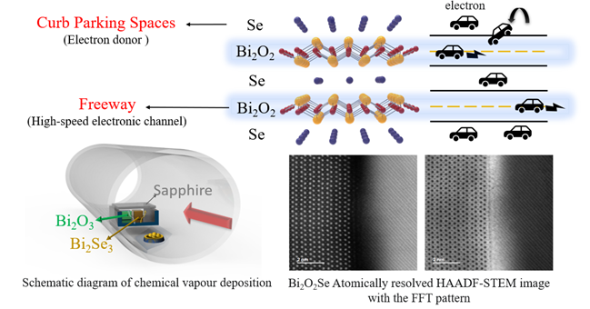 Figure 3. The laboratory uses low-pressure chemical vapor deposition to grow high-quality bismuth selenide and a schematic diagram of carrier transport.
Measured by angle-resolved photoemission spectroscopy (ARPES)(74)Clearly shows a single layer of Bi2O2Se is an indirect bandgap (0.8 eV) and has a very low in-plane effective electron mass (m* = 0.14 ± 0.02 m0 makes Bi2O2Se Hall components have an ultra-high electron mobility (>20,000 cm2V-1s-1and can observe the Shubnikov-de Haas (SdH) quantum oscillation phenomenon. Analyzed through optical absorption spectroscopy.(98)It can also confirm that the tunable optical bandgap depends on the change in thickness. As the thickness gradually decreases to a monolayer, the low residual carrier concentration and larger bandgap can provide good gate control capability. On the other hand, the phonon-dominated charge transport mechanism clarifies that the scattering of charge impurities can be effectively suppressed.(77)However, Bi2O2Se is not particularly sensitive to Raman spectroscopy analysis; in experimental aspects, only A1g(159 cm-1 ) and line defect Eu(~55 cm-1In the ) mode, it can be observed mainly due to the longitudinal optical phonon damping caused by small Raman scattering cross-section or high carrier concentration.(99)Interestingly, the effect of carrier concentration seems to be related to Bi2O2The changes in the surface structure of Se are related; Bi2O2Se single crystal is subjected to in-situ scanning tunneling microscopy (STM) in an ultra-high vacuum (UHV) chamber.(100)High-Resolution Transmission Electron Microscopy (HRTEM)(101)the measurement found Bi2O2The Se surface layer is peeled off, leaving only 50% of the atoms attached at the Se layer plane to [Bi.2O2]n2n+Upper or lower symmetric layers (zipper model), and exhibit a striped interwoven pattern between Se atoms and vacancies, which is attributed to the weak intrinsic electrostatic interactions [Bi2O2]n2n+/[Se]n2n-The native defects formed; surprisingly, due to the dimerization of Se atoms and the arrangement of Se vacancies, no covalent bonds are broken, and no bandgap states are generated; quantitative studies using X-ray photoelectron spectroscopy (XPS) also indirectly confirm the elemental dosage on the atomic structure surface (Bi 2:1 Se).(86)According to the above research, Se vacancies seem to be Bi2O2The main defects of Se(102)In most cases, the unshared electrons of Se atoms act as electron donors, resulting in Bi2O2The residual carriers of Se are too high, leading to a decrease in impedance.
The student surpasses the master.
Standing on the shoulders of giants broadens the horizon. Bi2O2Using silicon-based integrated circuits as a benchmark, vertical array FinFETs have been realized in the laboratory. Bismuth selenide semiconductors can be heated.(88)Plasma(87)or ultraviolet light-assisted oxygen activation method(89)The native oxide layer that creates a perfect lattice interface not only has a high dielectric constant but also possesses a lower defect density. Compared to silicon-based oxidation processes, it has a lower oxidation temperature and atomic-level interface quality. Moreover, it also has the ability to pattern lithography compatible with silicon-based processes.(82、90)In terms of selective area oxidation, etching, and growth, it is more flexible for component scale scaling compared to traditional transition metal dichalcogenides.
1. As integrated circuit components continue to shrink, there are forward-looking opportunities for atomic-level thin two-dimensional materials.
In the past nearly half a century, the microelectronics field has been dominated by silicon-based technology. As the continuous miniaturization of future dimensions progresses, the non-ideal effects under physical limit operations have restricted the feasibility of silicon technology for integration on the same plane. In recent years, low-dimensional materials have received widespread attention in the microelectronics field, such as the ballistic transport characteristics of indium selenide (InSe).(5)Carbon Nanotubes (CNT)(106)Ideal circular gate control capability, inert surface atomic layers without dangling bonds.(107)Low-power integrated circuit implementation, wafer-level microarray circuits and light-emitting diode development(108)The barrier length is less than 1 nanometer vertically MoS2transistor(109)high dielectric constant insulating layer(110)Currently, the fabrication of two-dimensional material devices largely inherits the technology of the silicon-based industry to develop novel physical property transistors (TSC-FET, FeFET, vdW-FET, NCFET, TFET, DSFET, Spin-FET) and memory devices (RRAM, FeRAM, ORRAM, PCM, STT-MRAM), and has the potential for synchronous logic memory and neuromorphic computing.
However, 2D materials face challenges in large-area CMOS integration. First: The atomic doping of 2D materials to achieve changes in conductivity needs to avoid excessive defects caused by large-scale structural damage.(57); Second: Directly synthesizing two-dimensional materials on silicon wafers will face contradictions and conflicts between high-temperature thermal budget (EBOL) and thin film quality; Third: Defects at the interface between two-dimensional material channels/insulators.(111)(hysteresis, leakage current, carrier mean free path hopping transport) will significantly reduce the performance of the component (the noise margin of the inverter.(112)Fourth: Inevitable contamination from residues after material transfer.(113)increasing the impedance value of the in-plane interconnect; fifth: lack of intuitive atomic and defect detection technology, affecting measurement uncertainty; sixth: the integration stacking of 3DIC, the metal in-plane interconnect requires high-precision alignment(114)Therefore, it is not easy for traditional two-dimensional semiconductors to replace silicon. Considering the maturity and benefits of the CMOS process, a more promising approach should focus on the integration of two-dimensional material devices with silicon technology (On-Silicon and With-Silicon), effectively integrating the advantages of two-dimensional materials with single atomic layers, and developing innovative VGAA and CFET architectures to further enhance the density of chip integration.
2. Milestones in the Large-Area Growth of Bismuth Selenide
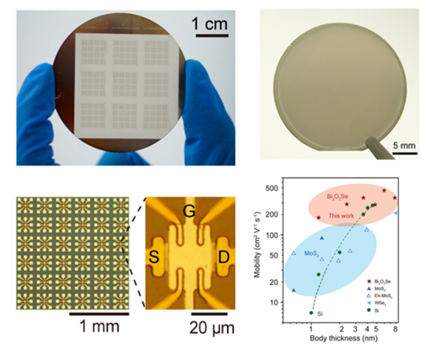
As shown in the example of Figure 4, the entire single crystal Bi2O2Se thin films exhibit good uniformity and are compatible with MoS2Compared to superior electron mobility; and the dependence of SdH quantum oscillation angle was also observed in Hall devices.(81)to confirm high-quality Bi2O2The formation of Se thin films.
3. The native oxide layer of bismuth selenide and its High-k characteristics
As CMOS transistors continue to shrink, the power consumption of the components decreases while the operating speed improves, further increasing the density of integrated circuits. It is worth mentioning that the native oxide layer (SiO) of silicon (Si) wafers...2), with easy growth, selective etching, excellent doping blocking function, and excellent passivation interface (Si/SiO2(and other advantages). It is a pity that SiO2When the thickness is below 10 nanometers, it is prone to dielectric breakdown, and as the thickness decreases, the leakage current gradually increases. In addition, the transistor's ability to control on/off depends on the dielectric properties, compared to SiO.2low dielectric constant (εr~3.9), the current mainstream method still uses ALD to deposit high-k dielectric HfO.2(εr~25) As a dielectric layer(115)However, HfO2It is difficult to form thin films through heterogeneous nucleation on the surface of two-dimensional materials without dangling bonds. Currently, the dielectric used for the heterojunctions of two-dimensional materials is hexagonal boron nitride (h-BN), due to its excellent interface with two-dimensional materials and extremely low interface trap density (below 10.10cm− 2eV− 1However, due to the easy contamination during the transfer process of h-BN materials and the occurrence of tunneling phenomena when the thickness is less than 5nm, leakage current situations arise.(116)Therefore, the so-called kindred spirits are hard to come by; silicon and silicon dioxide have complemented each other for many years, which is truly not easy.
Bi2O2Se is one of the very few two-dimensional semiconductors that possesses characteristics similar to silicon. In addition to high electron mobility, it can also form high-quality native oxide layers under easily controllable conditions. According to the thermal equilibrium phase diagram guidelines.(117)By controlling the oxygen content, the structure of the composition in the system can be changed, accompanied by corresponding changes in the energy gap, causing the semiconductor to transition to an insulator, resulting in Bi.2O2The native oxide layer exclusive to Se. Currently, the commonly used oxidation methods can be divided into three categories (Figure 5), corresponding to (1) plasma-assisted oxidation.(87)- Amorphous oxide layer, (2) high-temperature furnace thermal oxidation(88)-Co-bonded oxide layer (α phase), (3) UV-assisted oxidation(89)-Interlayer oxide layer (β phase).
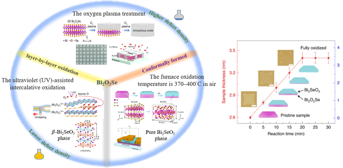
Figure 5. (Left) Bismuth selenide (Bi2O2Three oxidation methods of Se) (electrochemical-assisted oxidation, high-temperature furnace thermal oxidation, ultraviolet-assisted oxidation), (right) have controllable oxide layer numbers and selective etching.(87~89)
Plasma-assisted oxidation(87) uses O2Plasma, in Bi2O2Amorphous oxide Bi generated on the Se surface2SeOx), the amorphous oxide has a high dielectric constant characteristic (εr~22), low equivalent oxide thickness (EOT ~0.9nm), and shows the prospects of native oxides applied to gate control and resistive memory.
High temperature furnace thermal oxidation(88)The method is to heat the high-temperature furnace to 370~400.oC oxidizes in the atmospheric environment, Bi2O2Se (~1.09 eV) can be gradually transformed into α-Bi layer by layer.2SeO5(~3.9 eV), the characteristic of this structure is Bi2O2Se/α-Bi2SeO5Existing in the form of van der Waals interfaces, ensuring high-quality interface quality. Notably, the selective control of the number of oxide layers and etching is an important feature in the patterning technology of the semiconductor industry. Bi2O2Se/Bi2SeO5Exhibiting excellent transistor characteristics (field effect mobility of about 250 cm2V-1s-1The subthreshold swing is less than 75 mV/dec.-1and a larger inverter voltage gain (~150).
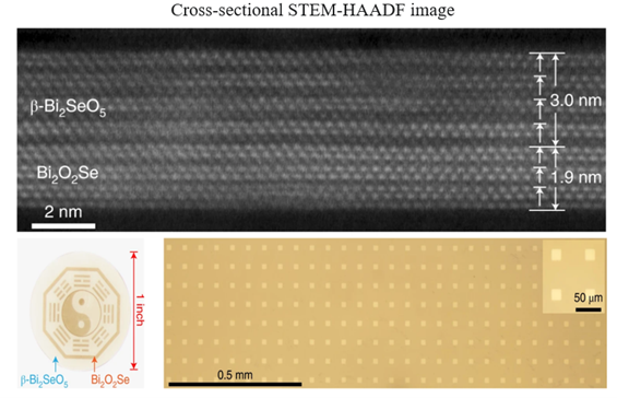
4. Selective area etching of bismuth selenide can pattern and promote the development of integrated circuits.
Similar to silicon processes, Bi2O2Se and Bi2SeO5The oxidation and etching of selected areas can also be done through lithography processes. The etching method can use piranha solution (Figure 7), which is a mixture obtained by diluting a specific ratio of sulfuric acid and hydrogen peroxide.(90)The piranha solution has a fast etching rate and can adjust the etching rate through dilution. On the other hand, Bi2O2The native oxide layer Bi obtained after oxidation of Se2SeO5hydrofluoric acid (HF)(88)Argon plasma etching(118)Hydrofluoric acid can effectively selectively etch Bi at an appropriate dilution ratio (0.2%).2SeO5Its etching selectivity is >100 (better than SiO)2Etching selectivity ratio ~40), indicating that during the etching of the oxide layer, the effect of bismuth selenide surpasses traditional silicon processes, giving it advantages that can compete with silicon-based semiconductor processes; the argon gas etching method can overcome the limitations of anisotropic etching such as wet etching, making it an excellent application in component processing.
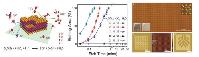
Figure 7.Bi2O2Sewet chemical etching to achieve patterning purposes(90)
5. The excellent performance of bismuth selenide field-effect transistors is expected to become a driving force for continuing Moore's Law.
Bi2O2Se has both high carrier mobility and native oxidation properties, making it a candidate material for the next generation of nanoscale transistors. Bi2O2The performance of Se transistors is mainly determined by the conditions of high-temperature vapor phase synthesis. It is expected that the transistor will have a high on-state current (Ion), it must have a high-quality material structure, which has a smaller effective mass and higher phonon energy, to enhance the mobility of carriers within the channel. As of the current record, Bi2O2Se surface vertical growth(85)At low temperatures (2K), an ultra-high Hall mobility of 160,000 cm can be obtained.2V–1s–1The high current density reached 1.33 mA μm.–1Due to not being affected by Bi2O2The difference in the thermal expansion and contraction coefficients between Se and the substrate reduces the linear defects and structural strain that cause wrinkles, effectively lowering the scattering of carriers at defect centers. A high current density in the ON state also implies the application of high-performance and low-power components.
This year, in 2023, an international team has successfully prepared Bi at the wafer scale.2O2Se/α-Bi2SeO5Epitaxial heterostructure two-dimensional FinFETs(16)As shown in Figure 8. Its advantages are (1) Bi2O2(1) Ultra-high carrier mobility; (2) Energy gap lower than silicon semiconductors; (3) Excellent chemical stability; (4) Controllable nucleation sites to achieve periodic array growth at specific locations and intervals; (5) Through the principle of lattice symmetry, the crystal plane orientation of the STO substrate can grow vertically and unidirectionally; (6) α-Bi2SeO5Native oxide layer with atomic-level flat interface, high dielectric constant characteristics, and precisely controllable atomic layer oxide thickness; (7) The oxide layer can be selectively etched in diluted hydrofluoric acid to serve as a perfect site for metal contacts. It is worth noting that Bi2O2Se/α-Bi2SeO5FinFETs have a carrier mobility of up to 1060 cm at room temperature.2V–1s–1Ultra-low cutoff current (Ioff)~1 pA μm−1 and on/off current ratio (ION/ IOFF) as high as 108Transistor performance comparable to Si FinFET, meeting the latest low power standards predicted by IRDS.
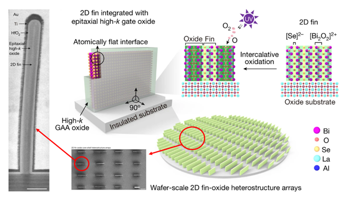
Figure 8. Bi2O2Se/Bi2SeO5FinFET(16)
Due to the atomic-level thickness and non-bonding characteristics of two-dimensional semiconductors, they have significant advantages in three-dimensional structures such as FinFETs, Vertical Gate-All-Around Field Effect Transistors (VGAA), and Vertical Complementary Field Effect Transistors (VCFET). The key lies in the dielectric materials, which must meet the requirements for high electrostatic gate control capability and high drive current density. As transistors continue to shrink below the 3-nanometer node, the limitations of dielectric materials hinder the development of silicon crystals.(119)Finding suitable gate dielectrics (high dielectric constant, atomically flat clean interface quality, and high-temperature operation tolerance) has become a current topic, which can avoid the occurrence of interface defect-induced electron capture scattering and leakage current. Here, the novel two-dimensional material "bismuth selenide Bi2O2Se has already broken the constraints of that limitation.
A hundred flowers bloom
In recent years, Bi2O2The research on Se has become an intriguing topic, with successive applications emerging like mushrooms after rain.(78~80). Since Bi2O2Interesting physical properties of semiconductors: smaller effective mass and faster carrier mobility.(85)tunable bandgap(120)Broad frequency light absorption and optical sensitivity(98)mechanical toughness, strong spin-orbit coupling(121)and the symmetry breaking caused by spontaneous lattice distortion(76)Control ability of doping and defect states(122)provides a variety of application platforms.
As mentioned above, Bi2O2The excellent performance of the field-effect transistor is a necessary condition for integrated circuits; also due to the intrinsic properties of the material, the effective mass of the charge carriers is low and the electron-phonon interaction is weak.(105)strong spin-orbit coupling, providing a more efficient platform for electronic transport. In addition, in the fields of optoelectronics, thermoelectrics, and ferroelectrics, Bi2O2Se also has fascinating research results and component applications.
1. Optoelectronics
photodetectors are Bi2O2One of the popular research projects in Se is the conversion between optical and electrical signals, which is mainly related to the optical frequency and the electronic transitions of the energy gap. For Bi2O2The bandgap of Se will change accordingly with thickness (bulk ~0.8 eV and monolayer ~2.12 eV)(74、120)Photocarrier relaxation phenomenon(98)And the ultra-high optical carrier mobility is a significant advantage for optical detection and its response. It has also led many optoelectronic experiments to propose various interesting mechanisms, such as: photothermal effect, photoconductive effect, grating effect, photovoltaic effect, greatly expanding the application range of optical switches, memory, logic devices, and more.
In 2017, the team led by Hailin Peng (90) first produced a 3x2 matrix Bi2O2Se photodetector, which displayed images through addressing and pixel recognition. At a wavelength of 532 nm and an incident power of about 0.1 nW, its intrinsic optical responsivity reached ~2000 AW-1, a value that surpasses all two-dimensional materials without added gratings. In the following year, the team utilized Bi2O2The low bandgap characteristics of Se and the excitation of optical carriers (123) can detect a photoresponsivity of ~65 AW-1 at an incident power of 0.1nW at a wavelength of 1200 nm. This high sensitivity is often attributed to the localized states (trap energy levels) within the material, which capture optical carriers and form photoconductive gain; a high detection rate (D* ~ 3.0×10⁹ Jones) and an extremely short response time of 1 ps. In 2019, the HuiMing Cheng team achieved the direct growth of high-quality single crystal Bi through gas-solid methods.2O2Se(93), at a wavelength of 660 nm, has a maximum optical responsivity of ~22,100 AW-1, with a detectivity of D* ~3.4×10¹⁵ Jones, and response time and relaxation time of 6 ms and 20 ms respectively; the possible reason is the few-layer Bi.2O2Se has weak interlayer electrostatic interaction and incomplete electric field screening, which will benefit the separation of electrons and holes, thereby enhancing photoelectric efficiency. In the same year, Yongbing Xu's team studied Bi2O2Se exhibits a broadband spectral response capability at room temperature (124) (360-1800nm wavelength range), with a responsivity of up to ~5×10^4 AW^-1 at a wavelength of 405 nm, an external quantum efficiency of 1.5×10^7%, and a detectivity of up to D*~3.4×10^12 Jones. Since the device has a top gate structure (Al2O3/Bi2O2Se), an increase in gate bias means that the Fermi level will approach the conduction band, which will enhance the photoconductive gain. The variation in optical response under different wavelengths and gate biases is attributed to the photovoltaic, photogate, and photothermal combined effects dominating the performance of the optical detector. In 2021, HuiMing Cheng's team grew Bi using the gas-solid-solid (VSS) method.2O2Se nanowire structure (86), at a wavelength of 660 nm, achieved the highest optical response value of ~9.19×10⁶ AW-1; single crystal Bi2O2The reduced carrier traps in the nanowire lead to decreased contamination of non-radiative recombination centers, demonstrating the high sensitivity characteristics of photodetectors.
In addition, using band modulation of heterostructures (Type II) to reduce dark current generation and promote charge space separation.(125)According to the Tianyou Zhaiw team(126)Research, PbSe/Bi2O2Se exhibits a detection capability for 2μm short infrared wavelengths and a faster response time of ~4ms; this result regulates the interface charge dipoles under different field effects, and under positive gate bias, the grating effect can more effectively separate the electron-hole pairs that dominate the current generation mechanism. Generally speaking, photodetectors have found radiation thermal effects in the measurement of optical responses at multiple wavelengths, and in the time evolution, photoconductivity will accompany the generation of radiation heat, that is, during the temperature rise, the phenomenon of thermal electron transition will also occur; therefore, Bi2O2Se exhibits a high radiative thermal coefficient (-31nA K-1) and high radiation thermal response rate (>320 AW-1)(127)is highly favored among candidate materials for future radiative thermal detectors.
2. Thermoelectric Field
Effectively converting thermal energy into electrical energy is a major trend in future energy utilization. The thermoelectric properties of materials are mainly measured by the figure of merit ZT (ZT=S2σT/κ), which was first prepared in bulk by the C. Uher team using the CVT method.2O2Se(128), via ZT=f(TThe variation of the temperature function (2~800 K) is used to estimate important parameters (κ thermal conductivity, σ electrical conductivity, S Seebeck coefficient), and indicates Bi2O2Se has a low intrinsic lattice thermal conductivity, and at high temperatures (800K) the ZT is about 0.2. Interestingly, Bi2O2The electronic performance characteristics of surface and bulk electrons are different. In addition to the easy introduction of extra dopant molecules between weak electrostatic layers, lattice distortions (Bi defects, Se vacancies) will also affect the behavior of electrons in the material. Furthermore, a trade-off must be made between "increasing electrical conductivity" and "reducing thermal conductivity" to enhance the quality factor ZT index.
Currently improving Bi2O2The mainstream method for Se thermoelectric performance mainly involves high-temperature solid-state reactions, using substitution (129) and doping (130) of atoms to increase carrier concentration, while enhancing lattice phonon scattering, thereby gradually suppressing the lattice thermal conductivity. The key lies in the Bi itself.2O2The high carrier mobility of Se allows for better conductivity with high carrier concentration. In addition, the modulation of the energy band and thickness will also enhance Bi.2O2Se thermoelectric properties; Zhenhua Ni's team studied Bi using Raman spectroscopy.2O2Se interface heat transfer (131) found that the in-plane thermal conductivity decreases with decreasing thickness. At the same time, the group velocity of phonons decreases, leading to increased surface scattering and strong non-ideality. The Liang Qiao team used first-principles calculations (132) to converge bilayer Bi.2O2The change in interlayer spacing of Se (3.65~ 3.35 Å) affects the effective density of states in the conduction band and valence band, which can effectively increase the ZT value. However, based on Bi2O2The thermoelectric properties of Se have rarely been developed and applied, only in 2020 did Ru Huang's team produce Bi.2O2The radiation heat sensor of the Se field-effect transistor (133) exhibits high sensitivity of 4.6 %K-1 and a temperature resolution of 1.5 mK at operating temperatures of 30 to 200 °C, and a sharp change in resistivity with temperature is observed; the results indicate that Bi2O2Se is expected to become a strong candidate for future high-performance thermoelectric devices and thermal sensors.
3. Ferroelectric Field
The spontaneous electric dipoles of ferroelectric materials occur under the influence of temperature changes or strain, exhibiting four characteristics (piezoelectric effect, phase transitions between paraelectric and ferroelectric states, changes in characteristic hysteresis loops, and high dielectric constants); in the absence of an electric field, the separation of positive/negative charges in the lattice forms electric dipoles. When a specific region has the same direction of spontaneous polarization, it is referred to as a ferroelectric domain; by applying a relatively positive/negative coercive electric field, the originally random polarization directions of the ferroelectric domains, which cancel each other out, gradually tend to become consistent, and when the electric field is removed, a residual polarization can be maintained; therefore, it is very suitable for applications in non-volatile storage devices (FeRAM, FeFET, FTJ).
As early as the 1940s, it was discovered that perovskite structures exhibit ferroelectric characteristics (PZT, BTO), but such oxide insulators are difficult to integrate into modern semiconductor processes, and the ferroelectric properties disappear when the thickness is below the critical thickness (∼ 24 Å).(134)This is due to the depolarization effect caused by the electric field generated by dipoles at the metal-ferroelectric interface. For the continuous miniaturization of semiconductor devices, the application of such materials is hindered. Recently, atomically thin ferroelectric materials have been discovered.(135)However, the vast majority of ferroelectric insulators face challenges in the stability of the ferroelectric state due to large band gaps and low carrier mobility. Due to the demand for technological updates in the silicon semiconductor industry, the team led by U. Böttger utilized metal-organic atomic layer deposition technology in 2011.(136)Doping hafnium oxide HfO in Si wafers2Thin film, HfO2The crystal will transition from a symmetric tetragonal structure to an orthorhombic phase when cooled down in temperature, thereby inducing two different polarization states of ferroelectricity and showing a significant piezoelectric response. Ongoing research by Sayeef Salahuddin's team successfully prepared 1nm thick Hf.0.8Zr0.2O2(HZO) ferroelectric layer(137)Experiments show that amplifying atomic displacements through regional strain (crystal distortion) can enhance the polarization phenomenon, which also means that: the breaking of inversion symmetry and the spontaneous polarization characteristics can maintain ferroelectric effects at the atomic scale.
Mechanical strain has an indispensable effect on two-dimensional materials, Bi2O2The high lattice symmetry of Se provides good conditions for fast electron transport. Another advantage is that under the influence of the electrostatic forces between layers, the symmetry can be affected by the planar sliding between layers and the main structure (Bi2O2The distortion and mechanical elastic strain factors are destroyed.(138)because it produces unique physical effects. Xiao Cheng Zeng and others have studied and pointed out(139), applying Bi2O2Se in-plane strain can not only induce polarization phenomena, but also cause changes in the band gap (indirectly becoming direct) under critical strain conditions, predicting Bi.2O2Se has ferroelectric and antiferroelectric properties. Kanishka Biswas's team used bismuth nitrate (Bi(NO3)3) and selenourea (SeC(NH2)2Mixed hydrolysis method(140)to synthesize ~2nm Bi2O2Se nanosheets have been shown through experiments that the spontaneous orthogonal deformation based on few-layer nanosheets breaks the local inversion symmetry, maintaining an ordered ferroelectric ground state even at room temperature. In addition, Wenbin Li's team, through theoretical calculations,(105),revealing Bi2O2The high mobility of Se can be attributed to the small elastic strain (1.7%) that promotes interlayer ferroelectric changes, thereby leading to a significant increase in the dielectric constant, which indirectly forms a protective effect on channel transport, effectively suppressing Coulomb scattering. Johnny C. Ho and others in their latest research.(76)indicates that the direction of polarization can be switched through the redistribution of opposite charges under positive/negative electric fields. Unlike traditional semiconductors, Bi2O2The transport channel of FeFET shows the presence of polarization bound charges, and the characteristics of ferroelectric hysteresis can be observed. In further experiments, a high piezoelectric constant was obtained, and Bi was utilized.2O2The ferroelectric polarization switching characteristics of FeFET can enhance the sensitivity of photodetectors. Based on the above, Bi2O2The properties of Se materials are expected to provide more diversified applications in various fields.
Throwing a brick to attract jade.
Currently, the research on bismuth selenide semiconductors is in full swing, but there are challenges to overcome, such as the large-area transfer technology of the materials and whether components with corresponding P-Type transport characteristics can be achieved through doping and phase changes is still an unknown. There is a strong desire to develop new transfer and growth technologies, and in the future, through industry-academia collaboration, it is hoped that the application of bismuth selenide integrated circuits can see the light of day.
Here, we thank MA-tek for their precise analytical technology that makes atomic structure imaging flawless (Figure 9). Through the acquisition of atomic information, the laboratory can efficiently complete the development of two-dimensional semiconductor materials and the application of components.
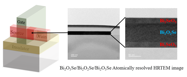
Figure 9. This laboratory uses UV ultraviolet light to form Bi through annular oxidation.2O5Se/Bi2O2Se/Bi2O5Se structure as FinFET application
Reference:
[1] Wang, S., Liu, X., & Zhou, P. (2022). The road for 2D semiconductors in the silicon age. Advanced Materials, 34(48), 2106886.
[2] Wang, X., Chen, X., Ma, J., Gou, S., Guo, X., Tong, L., ... & Bao, W. (2022). Pass‐Transistor Logic Circuits Based on Wafer‐Scale 2D Semiconductors. Advanced Materials, 2202472.
[3] Zhu, K., Wen, C., Aljarb, A. A., Xue, F., Xu, X., Tung, V., ... & Lanza, M. (2021). The development of integrated circuits based on two-dimensional materials. Nature Electronics, 4(11), 775-785.
[4] Novoselov, K. S., Geim, A. K., Morozov, S. V., Jiang, D. E., Zhang, Y., Dubonos, S. V., ... & Firsov, A. A. (2004). Electric field effect in atomically thin carbon films. Science, 306(5696), 666-669.
[5] Bandurin, D. A., Tyurnina, A. V., Yu, G. L., Mishchenko, A., Zólyomi, V., Morozov, S. V., ... & Cao, Y. (2017). High electron mobility, quantum Hall effect and anomalous optical response in atomically thin InSe. Nature nanotechnology, 12(3), 223-227.
[6] Wang, J. I., Yamoah, M. A., Li, Q., Karamlou, A. H., Dinh, T., Kannan, B., ... & Oliver, W. D. (2022). Hexagonal boron nitride as a low-loss dielectric for superconducting quantum circuits and qubits. Nature materials, 21(4), 398-403.
[7] Yankowitz, M., Chen, S., Polshyn, H., Zhang, Y., Watanabe, K., Taniguchi, T., ... & Dean, C. R. (2019). Tuning superconductivity in twisted bilayer graphene. Science, 363(6431), 1059-1064.
[8] Li, W., Gong, X., Yu, Z., Ma, L., Sun, W., Gao, S., ... & Wang, X. (2023). Approaching the quantum limit in two-dimensional semiconductor contacts. Nature, 613(7943), 274-279.
[9] Jiang, J., Xu, L., Qiu, C., & Peng, L. M. (2023). Ballistic two-dimensional InSe transistors. Nature, 1-6.
[10] Wang, X., Xiao, C., Park, H., Zhu, J., Wang, C., Taniguchi, T., ... & Xu, X. (2022). Light-induced ferromagnetism in moiré superlattices. Nature, 604(7906), 468-473.
[11] Li, J. X., Li, W. Q., Hung, S. H., Chen, P. L., Yang, Y. C., Chang, T. Y., ... & Liu, C. H. (2022). Electric control of valley polarization in monolayer WSe2 using a van der Waals magnet. Nature Nanotechnology, 17(7), 721-728.
[12] Shen, Y., Dong, Z., Sun, Y., Guo, H., Wu, F., Li, X., ... & Ren, T. L. (2022). The trend of 2D transistors toward integrated circuits: Scaling down and new mechanisms. Advanced Materials, 2201916.
[13] Akinwande, D., Huyghebaert, C., Wang, C. H., Serna, M. I., Goossens, S., Li, L. J., ... & Koppens, F. H. (2019). Graphene and two-dimensional materials for silicon technology. Nature, 573(7775), 507-518.
[14] Schram, T., Sutar, S., Radu, I., & Asselberghs, I. (2022). Challenges of Wafer‐Scale Integration of 2D Semiconductors for High‐Performance Transistor Circuits. Advanced Materials, 34(48), 2109796.
[15] Liu, C., Chen, H., Wang, S., Liu, Q., Jiang, Y. G., Zhang, D. W., ... & Zhou, P. (2020). Two-dimensional materials for next-generation computing technologies. Nature Nanotechnology, 15(7), 545-557.
[16] Tan, C., Yu, M., Tang, J., Gao, X., Yin, Y., Zhang, Y., ... & Peng, H. (2023). 2D fin field-effect transistors integrated with epitaxial high-k gate oxide. Nature, 1-7.
[17] Ayres, R. U., & Ayres, R. U. (2021). The transistor transition: 1945–1969. The History and Future of Technology: Can Technology Save Humanity from Extinction?, 425-466.
[18] Chapin, D. M., Fuller, C. S., & Pearson, G. L. (1954). A new silicon p‐n junction photocell for converting solar radiation into electrical power. Journal of applied physics, 25(5), 676-677.
[19] Atalla, M. M., Tannenbaum, E., & Scheibner, E. J. (1959). Stabilization of silicon surfaces by thermally grown oxides. Bell System Technical Journal, 38(3), 749-783.
[20] Huang, X., Lee, W. C., Kuo, C., Hisamoto, D., Chang, L., Kedzierski, J., ... & Hu, C. (1999, December). Sub 50-nm finfet: Pmos. In International Electron Devices Meeting 1999. Technical Digest (Cat. No. 99CH36318) (pp. 67-70). IEEE.
[21] Hisamoto, D., Lee, W. C., Kedzierski, J., Takeuchi, H., Asano, K., Kuo, C., ... & Hu, C. (2000). FinFET-a self-aligned double-gate MOSFET scalable to 20 nm. IEEE transactions on electron devices, 47(12), 2320-2325.
[22] Choi, Y. K., Lindert, N., Xuan, P., Tang, S., Ha, D., Anderson, E., ... & Hu, C. (2001, December). Sub-20 nm CMOS FinFET technologies. In International Electron Devices Meeting. Technical Digest (Cat. No. 01CH37224) (pp. 19-1). IEEE.
[23] Loubet, N., Hook, T., Montanini, P., Yeung, C. W., Kanakasabapathy, S., Guillom, M., ... & Khare, M. (2017, June). Stacked nanosheet gate-all-around transistor to enable scaling beyond FinFET. In 2017 Symposium on VLSI Technology (pp. T230-T231). IEEE.
[24] Das, S., Sebastian, A., Pop, E., McClellan, C. J., Franklin, A. D., Grasser, T., ... & Singh, R. (2021). Transistors based on two-dimensional materials for future integrated circuits. Nature Electronics, 4(11), 786-799.
[25] Liu, Y., Duan, X., Shin, H. J., Park, S., Huang, Y., & Duan, X. (2021). Promises and prospects of two-dimensional transistors. Nature, 591(7848), 43-53.
[26] Novoselov, K. S., Geim, A. K., Morozov, S. V., Jiang, D., Katsnelson, M. I., Grigorieva, I. V., ... & Firsov, A. A. (2005). Two-dimensional gas of massless Dirac fermions in graphene. Nature, 438(7065), 197-200.
[27] Geim, A. K., & Novoselov, K. S. (2007). The rise of graphene. Nature materials, 6(3), 183-191.
[28] Balandin, A. A., Ghosh, S., Bao, W., Calizo, I., Teweldebrhan, D., Miao, F., & Lau, C. N. (2008). Superior thermal conductivity of single-layer graphene. Nano letters, 8(3), 902-907.
[29] Liu, H., Neal, A. T., Zhu, Z., Luo, Z., Xu, X., Tománek, D., & Ye, P. D. (2014). Phosphorene: an unexplored 2D semiconductor with a high hole mobility. ACS nano, 8(4), 4033-4041.
[30] Vogt, P., De Padova, P., Quaresima, C., Avila, J., Frantzeskakis, E., Asensio, M. C., ... & Le Lay, G. (2012). Silicene: compelling experimental evidence for graphenelike two-dimensional silicon. Physical review letters, 108(15), 155501.
[31] Acun, A., Zhang, L., Bampoulis, P., Farmanbar, M. V., van Houselt, A., Rudenko, A. N., ... & Zandvliet, H. J. (2015). Germanene: the germanium analogue of graphene. Journal of physics: Condensed matter, 27(44), 443002.
[32] Ranjan, P., Lee, J. M., Kumar, P., & Vinu, A. (2020). Borophene: New sensation in flatland. Advanced Materials, 32(34), 2000531.
[33] Dean, C. R., Young, A. F., Meric, I., Lee, C., Wang, L., Sorgenfrei, S., ... & Hone, J. (2010). Boron nitride substrates for high-quality graphene electronics. Nature nanotechnology, 5(10), 722-726.
[34] Chen, T. A., Chuu, C. P., Tseng, C. C., Wen, C. K., Wong, H. S. P., Pan, S., ... & Li, L. J. (2020). Wafer-scale single-crystal hexagonal boron nitride monolayers on Cu (111). Nature, 579(7798), 219-223.
[35] Bandurin, D. A., Tyurnina, A. V., Yu, G. L., Mishchenko, A., Zólyomi, V., Morozov, S. V., ... & Cao, Y. (2017). High electron mobility, quantum Hall effect and anomalous optical response in atomically thin InSe. Nature nanotechnology, 12(3), 223-227.
[36] Novoselov, K. S., Mishchenko, A., Carvalho, A., & Castro Neto, A. H. (2016). 2D materials and van der Waals heterostructures. Science, 353(6298), aac9439.
[37] Manzeli, S., Ovchinnikov, D., Pasquier, D., Yazyev, O. V., & Kis, A. (2017). 2D transition metal dichalcogenides. Nature Reviews Materials, 2(8), 1-15.
[38] Choi, W., Choudhary, N., Han, G. H., Park, J., Akinwande, D., & Lee, Y. H. (2017). Recent development of two-dimensional transition metal dichalcogenides and their applications. Materials Today, 20(3), 116-130.
[39] Wang, Q. H., Kalantar-Zadeh, K., Kis, A., Coleman, J. N., & Strano, M. S. (2012). Electronics and optoelectronics of two-dimensional transition metal dichalcogenides. Nature nanotechnology, 7(11), 699-712.
[40] Radisavljevic, B., Radenovic, A., Brivio, J., Giacometti, V., & Kis, A. (2011). Single-layer MoS2 transistors. Nature nanotechnology, 6(3), 147-150.
[41] Ross, J. S., Klement, P., Jones, A. M., Ghimire, N. J., Yan, J., Mandrus, D. G., ... & Xu, X. (2014). Electrically tunable excitonic light-emitting diodes based on monolayer WSe2 p–n junctions. Nature nanotechnology, 9(4), 268-272.
[42] Qian, F., Bu, X., Wang, J., Mao, J., Han, S. T., & Zhou, Y. (2022). Transistors and logic circuits enabled by 2D transition metal dichalcogenides: a state-of-the-art survey. Journal of Materials Chemistry C.
[43] Wu, M., Xiao, Y., Zeng, Y., Zhou, Y., Zeng, X., Zhang, L., & Liao, W. (2021). Synthesis of two‐dimensional transition metal dichalcogenides for electronics and optoelectronics. InfoMat, 3(4), 362-396.
[44] Sangwan, V. K., Jariwala, D., Kim, I. S., Chen, K. S., Marks, T. J., Lauhon, L. J., & Hersam, M. C. (2015). Gate-tunable memristive phenomena mediated by grain boundaries in single-layer MoS2. Nature nanotechnology, 10(5), 403-406.
[45] Wang, Y., Kim, J. C., Li, Y., Ma, K. Y., Hong, S., Kim, M., ... & Chhowalla, M. (2022). P-type electrical contacts for 2D transition-metal dichalcogenides. Nature, 610(7930), 61-66.
[46] Zhang, K., Ding, C., Pan, B., Wu, Z., Marga, A., Zhang, L., ... & Huang, S. (2021). Visualizing van der Waals epitaxial growth of 2D heterostructures. Advanced Materials, 33(45), 2105079.
[47] Jariwala, D., Marks, T. J., & Hersam, M. C. (2017). Mixed-dimensional van der Waals heterostructures. Nature materials, 16(2), 170-181.
[48] Li, M. Y., Chen, C. H., Shi, Y., & Li, L. J. (2016). Heterostructures based on two-dimensional layered materials and their potential applications. Materials Today, 19(6), 322-335.
[49] Choi, S. H., Yun, S. J., Won, Y. S., Oh, C. S., Kim, S. M., Kim, K. K., & Lee, Y. H. (2022). Large-scale synthesis of graphene and other 2D materials towards industrialization. Nature Communications, 13(1), 1484.
[50] Wang, S., Liu, X., Xu, M., Liu, L., Yang, D., & Zhou, P. (2022). Two-dimensional devices and integration towards the silicon lines. Nature Materials, 21(11), 1225-1239.
[51] Fiori, G., Bonaccorso, F., Iannaccone, G., Palacios, T., Neumaier, D., Seabaugh, A., ... & Colombo, L. (2014). Electronics based on two-dimensional materials. Nature nanotechnology, 9(10), 768-779.
[52] Liu, C., Chen, H., Wang, S., Liu, Q., Jiang, Y. G., Zhang, D. W., ... & Zhou, P. (2020). Two-dimensional materials for next-generation computing technologies. Nature Nanotechnology, 15(7), 545-557.
[53] Chen, S., Mahmoodi, M. R., Shi, Y., Mahata, C., Yuan, B., Liang, X., ... & Lanza, M. (2020). Wafer-scale integration of two-dimensional materials in high-density memristive crossbar arrays for artificial neural networks. Nature Electronics, 3(10), 638-645.
[54] Migliato Marega, G., Zhao, Y., Avsar, A., Wang, Z., Tripathi, M., Radenovic, A., & Kis, A. (2020). Logic-in-memory based on an atomically thin semiconductor. Nature, 587(7832), 72-77.
[55] 5Lanza, M., Sebastian, A., Lu, W. D., Le Gallo, M., Chang, M. F., Akinwande, D., ... & Roldan, J. B. (2022). Memristive technologies for data storage, computation, encryption, and radio-frequency communication. Science, 376(6597), eabj9979.
[56] Liu, Y., Duan, X., Shin, H. J., Park, S., Huang, Y., & Duan, X. (2021). Promises and prospects of two-dimensional transistors. Nature, 591(7848), 43-53.
[57] Waltl, M., Knobloch, T., Tselios, K., Filipovic, L., Stampfer, B., Hernandez, Y., ... & Grasser, T. (2022). Perspective of 2D integrated electronic circuits: Scientific pipe dream or disruptive technology?. Advanced Materials, 34(48), 2201082.
[58] Zhang, Y., Yao, Y., Sendeku, M. G., Yin, L., Zhan, X., Wang, F., ... & He, J. (2019). Recent progress in CVD growth of 2D transition metal dichalcogenides and related heterostructures. Advanced materials, 31(41), 1901694.
[59] Knobloch, T., Illarionov, Y. Y., Ducry, F., Schleich, C., Wachter, S., Watanabe, K., ... & Grasser, T. (2021). The performance limits of hexagonal boron nitride as an insulator for scaled CMOS devices based on two-dimensional materials. Nature Electronics, 4(2), 98-108.
[60] Ma, D., Li, T., Yuan, D., He, C., Lu, Z., Lu, Z., ... & Wang, Y. (2018). The role of the intrinsic Se and In vacancies in the interaction of O2 and H2O molecules with the InSe monolayer. Applied Surface Science, 434, 215-227.
[61] Dai, Z., Liu, L., & Zhang, Z. (2019). Strain engineering of 2D materials: issues and opportunities at the interface. Advanced Materials, 31(45), 1805417.
[62] Hu, Z., Wu, Z., Han, C., He, J., Ni, Z., & Chen, W. (2018). Two-dimensional transition metal dichalcogenides: interface and defect engineering. Chemical Society Reviews, 47(9), 3100-3128.
[63] Rhodes, D., Chae, S. H., Ribeiro-Palau, R., & Hone, J. (2019). Disorder in van der Waals heterostructures of 2D materials. Nature materials, 18(6), 541-549.
[64] Jung, Y., Choi, M. S., Nipane, A., Borah, A., Kim, B., Zangiabadi, A., ... & Teherani, J. T. (2019). Transferred via contacts as a platform for ideal two-dimensional transistors. Nature Electronics, 2(5), 187-194.
[65] Late, D. J., Liu, B., Matte, H. R., Dravid, V. P., & Rao, C. N. R. (2012). Hysteresis in single-layer MoS2 field effect transistors. ACS nano, 6(6), 5635-5641.
[66] Yang, S., Liu, K., Xu, Y., Liu, L., Li, H., & Zhai, T. (2023). Gate Dielectrics Integration for 2D Electronics: Challenges, Advances, and Outlook. Advanced Materials, 35(18), 2207901.
[67] Schram, T., Sutar, S., Radu, I., & Asselberghs, I. (2022). Challenges of wafer‐scale integration of 2D semiconductors for high‐performance transistor circuits. Advanced Materials, 34(48), 2109796
[68] Zhang, K., & Robinson, J. (2019). Doping of two-dimensional semiconductors: A rapid review and outlook. MRS Advances, 4(51-52), 2743-2757.
[69] Jiang, J., Parto, K., Cao, W., & Banerjee, K. (2019). Ultimate monolithic-3D integration with 2D materials: rationale, prospects, and challenges. IEEE Journal of the Electron Devices Society, 7, 878-887.
[70] Oppermann, H., Göbel, H., Schadow, H., Vassilev, V., & Markova‐Deneva, I. (1996). Thermochemical Investigations of the System Bi/Se/OI The Phase Triangle Bi2Se3/Bi2O2Se/Se. Journal of Inorganic and General Chemistry, 622(12), 2115-2118.
[71] Wu, J., Tan, C., Tan, Z., Liu, Y., Yin, J., Dang, W., ... & Peng, H. (2017). Controlled synthesis of high-mobility atomically thin bismuth oxyselenide crystals. Nano letters, 17(5), 3021-3026.
[72] Wu, J., Qiu, C., Fu, H., Chen, S., Zhang, C., Dou, Z., ... & Peng, H. (2018). Low residual carrier concentration and high mobility in 2D semiconducting Bi2O2Se. Nano Letters, 19(1), 197-202.
[73] Ding, X., Li, M., Chen, P., Zhao, Y., Zhao, M., Leng, H., ... & Qiao, L. (2022). Bi2O2Se: A rising star for semiconductor devices. Matter, 5(12), 4274-4314.
[74] Wu, J., Yuan, H., Meng, M., Chen, C., Sun, Y., Chen, Z., ... & Peng, H. (2017). High electron mobility and quantum oscillations in non-encapsulated ultrathin semiconducting Bi2O2Se. Nature Nanotechnology, 12(6), 530-534.
[75] Meng, M., Huang, S., Tan, C., Wu, J., Jing, Y., Peng, H., & Xu, H. Q. (2018). Strong spin–orbit interaction and magnetotransport in semiconductor Bi2O2Se nanoplates. Nanoscale, 10(6), 2704-2710.
[76] Wang, W., Meng, Y., Zhang, Y., Zhang, Z., Wang, W., Lai, Z., ... & Ho, J. C. (2023). Electrically Switchable Polarization in Bi2O2Se Ferroelectric Semiconductors. Advanced Materials, 35(12),2210854.
[77] Fu, H., Wu, J., Peng, H., & Yan, B. (2018). Self-modulation doping effect in the high-mobility layered semiconductor Bi2O2Se. Physical Review B, 97(24), 241203.
[78] Sun, Y., Zhang, J., Ye, S., Song, J., & Qu, J. (2020). Progress report on property, preparation, and application of Bi2O2Se. Advanced Functional Materials, 30(49), 2004480.
[79] Chen, W., Zhang, R., Sun, Y., Wang, J., Fan, Y., & Liu, B. (2022). Preparation, properties, and electronic applications of 2D Bi2O2Se. Advanced Powder Materials, 100080.
[80] Li, T., & Peng, H. (2021). 2D Bi2O2Se: an emerging material platform for the next-generation electronic industry. Accounts of Materials Research, 2(9), 842-853.
[81] Zhou, X., Liang, Y., Fu, H., Zhu, R., Wang, J., Cong, X., ... & Peng, H. (2022). Step‐Climbing Epitaxy of Layered Materials with Giant Out‐of‐Plane Lattice Mismatch. Advanced Materials, 34(42), 2202754.
[82] Tan, C., Tang, M., Wu, J., Liu, Y., Li, T., Liang, Y., ... & Peng, H. (2019). Wafer-scale growth of single-crystal 2D semiconductor on perovskite oxides for high-performance transistors. Nano Letters, 19(3), 2148-2153.
[83] Song, Y., Li, Z., Li, H., Tang, S., Mu, G., Xu, L., ... & Jiang, M. (2020). Epitaxial growth and characterization of high quality Bi2O2Se thin films on SrTiO3 substrates by pulsed laser deposition. Nanotechnology, 31(16), 165704.
[84] Yang, J., Jiang, R., Chen, C., Chen, J., Cao, Z., Li, Y., ... & Chu, J. (2023). Exploration on the growth of Bi2O2Se films and nanosheet by an ALD-assisted CVD method. Journal of Materials Science: Materials in Electronics, 34(9), 788.
[85] Tan, C., Jiang, J., Wang, J., Yu, M., Tu, T., Gao, X., ... & Peng, H. (2022). Strain-free layered semiconductors for 2D transistors with on-state current density exceeding 1.3 mA μm–1. Nano Letters, 22(9), 3770-3776.
[86] Khan, U., Tang, L., Ding, B., Yuting, L., Feng, S., Chen, W., ... & Cheng, H. M. (2021). Catalyst‐free growth of atomically thin Bi2O2Se nanoribbons for high‐performance electronics and optoelectronics. Advanced Functional Materials, 31(31), 2101170.
[87] Tu, T., Zhang, Y., Li, T., Yu, J., Liu, L., Wu, J., ... & Peng, H. (2020). Uniform high-k amorphous native oxide synthesized by oxygen plasma for top-gated transistors. Nano Letters, 20(10), 7469-7475.
[88] Li, T., Tu, T., Sun, Y., Fu, H., Yu, J., Xing, L., ... & Peng, H. (2020). A native oxide high-κ gate dielectric for two-dimensional electronics. Nature Electronics, 3(8), 473-478.
[89] Zhang, Y., Yu, J., Zhu, R., Wang, M., Tan, C., Tu, T., ... & Peng, H. (2022). A single-crystalline native dielectric for two-dimensional semiconductors with an equivalent oxide thickness below 0.5 nm. Nature Electronics, 5(10), 643-649.
[90] Wu, J., Liu, Y., Tan, Z., Tan, C., Yin, J., Li, T., ... & Peng, H. (2017). Chemical Patterning of High‐Mobility Semiconducting 2D Bi2O2Se Crystals for Integrated Optoelectronic Devices. Advanced Materials, 29(44), 1704060.
[91] Boller, H. (1973). The crystal structure of Bi 2 O 2 Se. Monatshefte für Chemie/Chemical Monthly, 104, 916-919.
[92] Li, X., Cai, W., An, J., Kim, S., Nah, J., Yang, D., ... & Ruoff, R. S. (2009). Large-area synthesis of high-quality and uniform graphene films on copper foils. science, 324(5932), 1312-1314.
[93] Khan, U., Luo, Y., Tang, L., Teng, C., Liu, J., Liu, B., & Cheng, H. M. (2019). Controlled vapor–solid deposition of millimeter‐size single crystal 2D Bi2O2Se for high‐performance phototransistors. Advanced Functional Materials, 29(14), 1807979.
[94] Yang, X., Zhang, Q., Song, Y., Fan, Y., He, Y., Zhu, Z., ... & Novoselov, K. (2021). High mobility two-dimensional bismuth oxyselenide single crystals with large grain size grown by reverse-flow chemical vapor deposition. ACS Applied Materials & Interfaces, 13(41), 49153-49162.
[95] Zou, X., Sun, Y., & Wang, C. (2022). Horizontally Self‐Standing Growth of Bi2O2Se Achieving Optimal Optoelectric Properties. Small Methods, 6(8), 2200347.
[96] Wu, Z., Liu, G., Wang, Y., Yang, X., Wei, T., Wang, Q., ... & Zhu, J. (2019). Seed‐Induced Vertical Growth of 2D Bi2O2Se Nanoplates by Chemical Vapor Transport. Advanced Functional Materials, 29(50), 1906639.
[97] Liang, Y., Chen, Y., Sun, Y., Xu, S., Wu, J., Tan, C., ... & Peng, H. (2019). Molecular beam epitaxy and electronic structure of atomically thin oxyselenide films. Advanced Materials, 31(39), 1901964.
[98] Zhu, C., Tong, T., Liu, Y., Meng, Y., Nie, Z., Wang, X., ... & Wang, F. (2018). Observation of bimolecular recombination in high mobility semiconductor Bi2O2Se using ultrafast spectroscopy. Applied Physics Letters, 113(6).
[99] Kim, U. J., Nam, S. H., Seo, J., Yang, M., Fu, Q., Liu, Z., ... & Hahm, M. G. (2022). Visualizing Line Defects in non-van der Waals Bi2O2Se Using Raman Spectroscopy. ACS nano, 16(3), 3637-3646.
[100] Chen, C., Wang, M., Wu, J., Fu, H., Yang, H., Tian, Z., ... & Chen, Y. (2018). Electronic structures and unusually robust bandgap in an ultrahigh-mobility layered oxide semiconductor, Bi2O2Se. Science advances, 4(9), eaat8355.
[101] Wei, Q., Li, R., Lin, C., Han, A., Nie, A., Li, Y., ... & Huang, W. (2019). Quasi-two-dimensional se-terminated bismuth oxychalcogenide (Bi2O2Se). ACS nano, 13(11), 13439-13444.
[102] Li, H., Xu, X., Zhang, Y., Gillen, R., Shi, L., & Robertson, J. (2018). Native point defects of semiconducting layered Bi2O2Se. Scientific Reports, 8(1), 10920.
[103] Ge, Z., Zhao, W., Yuan, S., Gao, Z., Hao, C., Ma, H., ... & Guo, W. (2023). Effect of surface Se concentration on stability and electronic structure of monolayer Bi2O2Se. Applied Surface Science, 611, 155528.
[104] Tong, T., Zhang, M., Chen, Y., Li, Y., Chen, L., Zhang, J., ... & Zhang, R. (2018). Ultrahigh Hall mobility and suppressed backward scattering in layered semiconductor Bi2O2Se. Applied Physics Letters, 113(7).
[105] Zhu, Z., Yao, X., Zhao, S., Lin, X., & Li, W. (2022). Giant modulation of the electron mobility in semiconductor Bi2O2Se via incipient ferroelectric phase transition. Journal of the American Chemical Society, 144(10), 4541-4549.
[106] Qiu, C., Zhang, Z., Xiao, M., Yang, Y., Zhong, D., & Peng, L. M. (2017). Scaling carbon nanotube complementary transistors to 5-nm gate lengths. Science, 355(6322), 271-276.
[107] Cui, X., Lee, G. H., Kim, Y. D., Arefe, G., Huang, P. Y., Lee, C. H., ... & Hone, J. (2015). Multi-terminal transport measurements of MoS2 using a van der Waals heterostructure device platform. Nature nanotechnology, 10(6), 534-540.
[108] Hwangbo, S., Hu, L., Hoang, A. T., Choi, J. Y., & Ahn, J. H. (2022). Wafer-scale monolithic integration of full-colour micro-LED display using MoS2 transistor. Nature Nanotechnology, 17(5), 500-506.
[109] Wu, F., Tian, H., Shen, Y., Hou, Z., Ren, J., Gou, G., ... & Ren, T. L. (2022). Vertical MoS2 transistors with sub-1-nm gate lengths. Nature, 603(7900), 259-264.
[110] Yang, A. J., Han, K., Huang, K., Ye, C., Wen, W., Zhu, R., ... & Renshaw Wang, X. (2022). Van der Waals integration of high-κ perovskite oxides and two-dimensional semiconductors. Nature Electronics, 5(4), 233-240.
[111] Lu, Z., Chen, Y., Dang, W., Kong, L., Tao, Q., Ma, L., ... & Liu, Y. (2023). Wafer-scale high-κ dielectrics for two-dimensional circuits via van der Waals integration. Nature Communications, 14(1), 2340.
[55] Lanza, M., Sebastian, A., Lu, W. D., Le Gallo, M., Chang, M. F., Akinwande, D., ... & Roldan, J. B. (2022). Memristive technologies for data storage, computation, encryption, and radio-frequency communication. Science, 376(6597), eabj9979.
[112] Wachter, S., Polyushkin, D. K., Bethge, O., & Mueller, T. (2017). A microprocessor based on a two-dimensional semiconductor. Nature communications, 8(1), 14948.
[113] Liu, X., Huang, K., Zhao, M., Li, F., & Liu, H. (2019). A modified wrinkle-free MoS2 film transfer method for large area high mobility field-effect transistor. Nanotechnology, 31(5), 055707.
[114] Schram, T., Sutar, S., Radu, I., & Asselberghs, I. (2022). Challenges of wafer‐scale integration of 2D semiconductors for high‐performance transistor circuits. Advanced Materials, 34(48), 2109796.
[115] Li, W., Zhou, J., Cai, S., Yu, Z., Zhang, J., Fang, N., ... & Wang, X. (2019). Uniform and ultrathin high-κ gate dielectrics for two-dimensional electronic devices. Nature Electronics, 2(12), 563-571.
[116] Illarionov, Y. Y., Knobloch, T., Jech, M., Lanza, M., Akinwande, D., Vexler, M. I., ... & Grasser, T. (2020). Insulators for 2D nanoelectronics: the gap to bridge. Nature Communications, 11(1), 3385.
[117] Xu, X., Li, B., & Li, H. (2021). Native O and Se Vacancy Defects in Bi2O5Se, Bi2O9Se3, and Bi2O10Se3 Dielectrics for Nanoelectronics. physica status solidi (RRL)–Rapid Research Letters, 15(2), 2000540.
[118] Gao, M., Wei, W., Han, T., Li, B., Zeng, Z., Luo, L., & Zhu, C. (2022). Defect Engineering in Thickness-Controlled Bi2O2Se-Based Transistors by Argon Plasma Treatment. ACS Applied Materials & Interfaces, 14(13), 15370-15380.
[119] Theis, T. N., & Wong, H. S. P. (2017). The end of moore's law: A new beginning for information technology. Computing in science & engineering, 19(2), 41-50.
[120] Zhu, X. L., Liu, P. F., Xie, G., & Wang, B. T. (2019). First-principles study of thermal transport properties in the two-and three-dimensional forms of Bi 2 O 2 Se. Physical Chemistry Chemical Physics, 21(21), 10931-10938.
[121] Gao, J., Lu, F., Liu, X., Deng, J., Zhang, X., Sun, Z., ... & Ding, X. (2022). Detection and tuning of spin-orbit interactions on inclined-grown Bi2O2Se nanoplates. Applied Physics Letters, 120(1), 013105.
[122] Liu, J., Yang, F., Lu, J., Ye, S., Guo, H., Nie, H., ... & Ni, Z. (2022). High output mode-locked laser empowered by defect regulation in 2D Bi2O2Se saturable absorber. Nature communications, 13(1), 3855.
[123] Yin, J., Tan, Z., Hong, H., Wu, J., Yuan, H., Liu, Y., ... & Peng, H. (2018). Ultrafast and highly sensitive infrared photodetectors based on two-dimensional oxyselenide crystals. Nature communications, 9(1), 3311.
[124] Tong, T., Chen, Y., Qin, S., Li, W., Zhang, J., Zhu, C., ... & Xu, Y. (2019). Sensitive and ultrabroadband phototransistor based on two‐dimensional Bi2O2Se nanosheets. Advanced Functional Materials, 29(50), 1905806.
[125] Yang, T., Li, X., Wang, L., Liu, Y., Chen, K., Yang, X., ... & Shan, C. X. (2019). Broadband photodetection of 2D Bi2O2Se–MoSe2 heterostructure. Journal of Materials Science, 54(24), 14742-14751.
[126] Luo, P., Zhuge, F., Wang, F., Lian, L., Liu, K., Zhang, J., & Zhai, T. (2019). PbSe quantum dots sensitized high-mobility Bi2O2Se nanosheets for high-performance and broadband photodetection beyond 2 μm. ACS nano, 13(8), 9028-9037.
[127] Yang, H., Tan, C., Deng, C., Zhang, R., Zheng, X., Zhang, X., ... & Qin, S. (2019). Bolometric effect in Bi2O2Se photodetectors. Small, 15(43), 1904482.
[128] Ruleova, P., Drasar, C., Lostak, P., Li, C. P., Ballikaya, S., & Uher, C. (2010). Thermoelectric properties of Bi2O2Se. Materials Chemistry and Physics, 119(1-2), 299-302.
[129] Pan, L., Zhao, Z., Yang, N., Xing, W., Zhang, J., Liu, Y., ... & Wang, Y. (2020). Effects of sulfur substitution for oxygen on the thermoelectric properties of Bi2O2Se. Journal of the European Ceramic Society, 40(15), 5543-5548.
[130] Tan, X., Liu, Y., Liu, R., Zhou, Z., Liu, C., Lan, J. L., ... & Nan, C. W. (2019). Synergistical Enhancement of Thermoelectric Properties in n‐Type Bi2O2Se by Carrier Engineering and Hierarchical Microstructure. Advanced Energy Materials, 9(31), 1900354.
[131] Yang, F., Wang, R., Zhao, W., Jiang, J., Wei, X., Zheng, T., ... & Ni, Z. (2019). Thermal transport and energy dissipation in two-dimensional Bi2O2Se. Applied Physics Letters, 115(19).
[132] Li, M., Wang, N., Jiang, M., Xiao, H., Zhang, H., Liu, Z., ... & Qiao, L. (2019). Improved thermoelectric performance of bilayer Bi 2 O 2 Se by the band convergence approach. Journal of Materials Chemistry C, 7(35), 11029-11039.
[133] Cai, Q., Liu, S., Du, M., Xu, L., Zhao, C., Tan, C., ... & Huang, R. (2020, December). Sub-10mK-Resolution Thermal-Bolometric Integrated FET-Type Sensors Based on Layered Bi2O2Se Semiconductor Nanosheets. In 2020 IEEE International Electron Devices Meeting (IEDM) (pp. 26-1). IEEE.
[134] Junquera, J., & Ghosez, P. (2003). Critical thickness for ferroelectricity in perovskite ultrathin films. Nature, 422(6931), 506-509.
[135] Yuan, S., Luo, X., Chan, H. L., Xiao, C., Dai, Y., Xie, M., & Hao, J. (2019). Room-temperature ferroelectricity in MoTe2 down to the atomic monolayer limit. Nature communications, 10(1), 1775.
[136] Böscke, T. S., Müller, J., Bräuhaus, D., Schröder, U., & Böttger, U. (2011). Ferroelectricity in hafnium oxide thin films. Applied Physics Letters, 99(10).
[137] Cheema, S. S., Kwon, D., Shanker, N., Dos Reis, R., Hsu, S. L., Xiao, J., ... & Salahuddin, S. (2020). Enhanced ferroelectricity in ultrathin films grown directly on silicon. Nature, 580(7804), 478-482.
[138] Cheng, T., Tan, C., Zhang, S., Tu, T., Peng, H., & Liu, Z. (2018). Raman spectra and strain effects in bismuth oxychalcogenides. The Journal of Physical Chemistry C, 122(34), 19970-19980.
[139] Wu, M., & Zeng, X. C. (2017). Bismuth oxychalcogenides: a new class of ferroelectric/ferroelastic materials with ultra high mobility. Nano Letters, 17(10), 6309-6314.
[140] Ghosh, T., Samanta, M., Vasdev, A., Dolui, K., Ghatak, J., Das, T., ... & Biswas, K. (2019). Ultrathin free-standing nanosheets of Bi2O2Se: room temperature ferroelectricity in self-assembled charged layered heterostructure. Nano letters, 19(8), 5703-5709.


