
Innovative Breakthroughs in Copper Hybrid Bonding Technology: Key Technologies for 3D Integrated Circuits and Advanced Packaging
Innovations in Copper Hybrid Bonding Technology:
Key Technologies for 3D Integrated Circuits and Advanced Packaging
Prof. Chen Kuan-Neng, Liu Yu-Lun
National Yang Ming Chiao Tung University Institute of Electronics
-
Introduction
Three-dimensional integrated circuit (3D IC) technology is gradually becoming a key technology driving innovation in the semiconductor industry. With the development of applications such as artificial intelligence (AI), high-performance computing (HPC), 5G communication, and the Internet of Things (IoT), the traditional Moore's Law has reached saturation, making the method of enhancing performance through planar miniaturization face physical limits. In contrast, 3D ICs break this limitation by vertically stacking multiple chips or wafers, achieving higher computing performance, lower power consumption, and tighter system integration. Compared to traditional 2D ICs, 3D ICs can significantly shorten the interconnection distance within and between chips, greatly reducing parasitic resistance and parasitic capacitance, thereby enhancing signal transmission speed, reducing power loss, and improving overall bandwidth, making them an ideal choice for applications such as high bandwidth memory (HBM), AI accelerators, and data centers. In addition, 3D IC technology can also promote heterogeneous integration, allowing components with different process nodes, different materials, or even different functions to work together within a single package. For example, integrating heterogeneous chips such as processors (CPU/GPU), memory (DRAM), radio frequency (RF), and sensors into a compact package not only enhances system performance but also optimizes costs and improves design flexibility.
As the demand for higher computational performance, lower latency, and more energy-efficient electronic components continues to grow, the semiconductor industry is rapidly advancing towards three-dimensional integrated circuit technology. To meet the need for lower power consumption and higher input/output (I/O) density, the interconnection technology of integrated circuits (IC) is constantly evolving. Traditionally, flip-chip technology uses solder bumps as the standard interconnection method between high-performance chips and packages, with a pitch typically exceeding 100 µm. However, this large pitch solder bump interconnection method suffers from parasitic resistance and parasitic capacitance effects, leading to signal attenuation and increased energy consumption, which further affects signal integrity and power efficiency, ultimately limiting the overall system performance. To enhance integration density and achieve high bandwidth memory (HBM) stacking and other advanced packaging applications, the industry has turned to microbump technology, which reduces the pitch to 10–50 µm. However, microbumps still face fundamental challenges such as electromigration (EM), increased contact resistance, and reliability issues caused by underfill, which hinder further miniaturization of interconnection technology.
To address these challenges, hybrid bonding technology has emerged as a breakthrough solution. This technology enables direct copper-to-copper bonding and dielectric-to-dielectric bonding at distances below 10 µm, eliminating the need for solder, significantly reducing parasitic effects in interconnections, and greatly enhancing signal integrity and power efficiency [5], [6]. Recent advancements in wafer-to-wafer (W2W) and die-to-wafer (D2W) hybrid bonding technology have pushed interconnection distances down to sub-micron levels, which is crucial for the realization of high-density three-dimensional system-on-chip (3D-SoC) architectures, and can further expand applications requiring high bandwidth and low latency data transmission, including artificial intelligence (AI) accelerators, data center architectures, and advanced mobile processors [7], [8]. Additionally, the excellent thermal stability and mechanical stability of hybrid bonding facilitate heterogeneous integration, allowing different materials and functional components to be seamlessly integrated into compact and high-performance system architectures [9].
Development trajectory
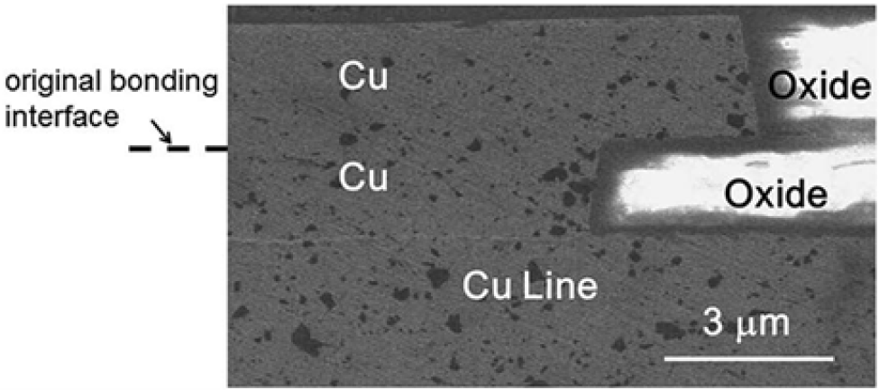
Hybrid bonding can be used to stack two structures, such as chips, wafers, and substrates, each composed of metal and surrounding dielectric materials. During the hybrid bonding process, the metal materials and dielectric materials are bonded separately. Although hybrid bonding is currently regarded as one of the ultimate technologies for 3D IC integration, the earliest 3D IC integration technology began with copper-to-copper (Cu-to-Cu) bonding technology. Between 1999 and 2002, the Reif research team at the Massachusetts Institute of Technology (MIT) proposed a wafer-level 3D integration scheme, which included the use of a carrier wafer (Si carrier), thinning technology, and direct copper-to-copper bonding, as shown in Figure 1 [1]. To avoid thermal damage to the components within the wafer, the maximum temperature for copper-to-copper bonding was limited to 400°C to comply with the thermal budget of CMOS processes. In 2001, Professor Chen Guan-neng demonstrated within the Reif team that copper-to-copper bonding could be successfully performed at 400°C, and its bonding interface completely disappeared, proving the feasibility of the technology [10]. As shown in Figure 2, the thermal compression bonding conditions were 400°C and 400 mbar for 30 minutes, followed by annealing at 400°C for 30 minutes in a nitrogen (N₂) environment [11]. This bonding temperature of 400°C was subsequently applied to the continuing development of hybrid bonding processes.
-
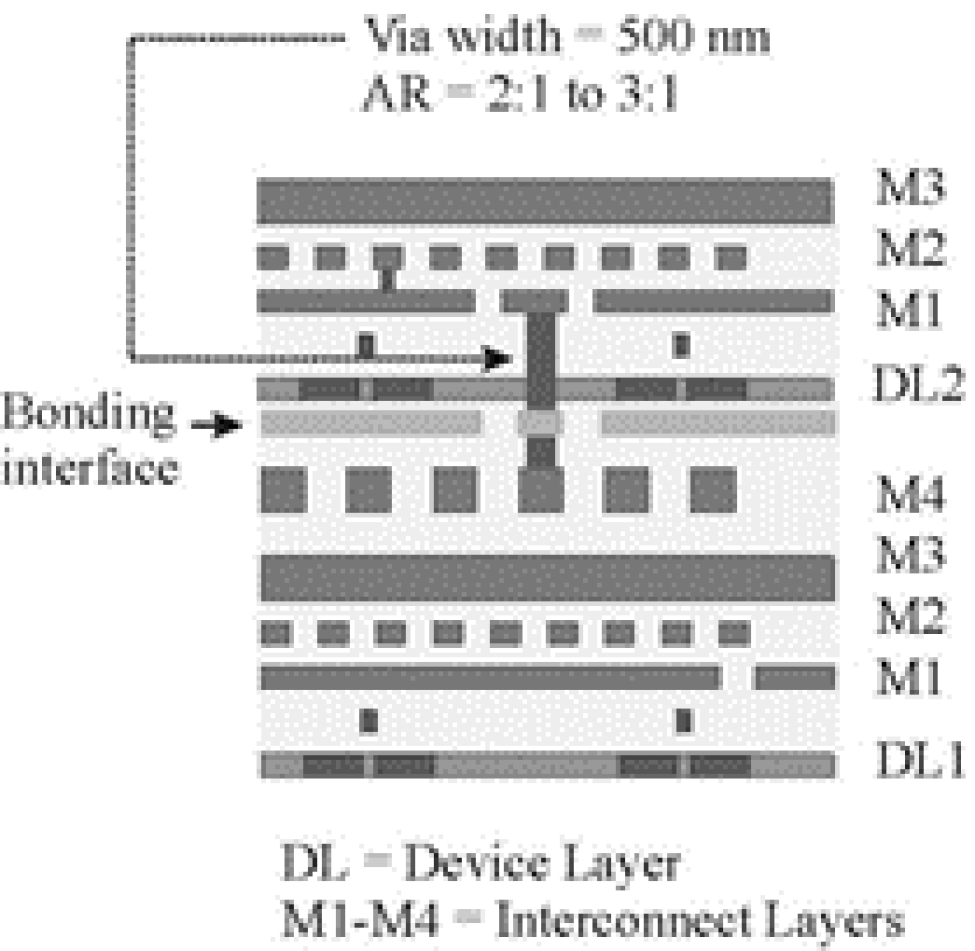
Figure 1. Example of three-dimensional integrated circuits [1]
-
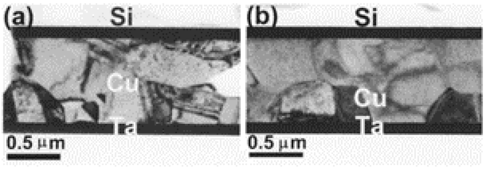
Figure 2. Image of the Cu-Cu bonding layer after 30 minutes of bonding [10]
Between 2000 and 2005, Professor Chen Guan-neng published a large number of studies on copper-to-copper bonding, including morphological evolution, bonding strength, bonding parameter criteria, and electrical properties [11-14]. Test results showed that the average contact resistance of a good copper-to-copper bonding structure is about 1×10⁻⁸ Ω−cm², with a minimum reaching 1.2×10⁻.9Ω−cm² [14]. In 2006, Professor Chen Guan-neng published a comprehensive study on copper-to-copper bonding during his time at IBM at the International Electron Devices Meeting (IEDM), covering structural design and pattern considerations [15]. However, in the original copper-to-copper bonding scheme, there were no other materials surrounding the copper, which could lead to potential reliability issues, such as copper corrosion or insufficient overall bonding strength. Although these issues can be addressed by using underfill to fill the gaps at the copper bonding interface, this method is extremely challenging due to the height of the copper pads being only a few microns. Furthermore, the underfill method is only applicable to chip-level bonding and not to wafer-level bonding.
To address these issues, researchers proposed an intuitive solution by adding surrounding dielectric materials before copper-to-copper bonding. Suitable dielectric materials include silicon dioxide (SiO₂) or polymer materials. The ideal bonding scenario is to achieve both copper-to-copper and dielectric-to-dielectric bonding simultaneously. In 2005, RPI's Gutmann and Lu team successfully demonstrated a 200mm wafer-level Cu/BCB (benzocyclobutene) thermocompression bonding technology, applying a pressure of 10,000 N at 250°C for 30 minutes, followed by heating to 350°C for an additional 30 minutes, as shown in Figure 3 [16]. This technology was officially named "Hybrid Bonding" in the same year [17], and since then, researchers have begun to develop ideal hybrid bonding techniques based on Cu/Polymer and Cu/SiO₂ structures. To leverage the compliance of polymers, IBM scientists developed a "Lock-and-Key" hybrid bonding structure, where the copper pad/copper pillar structure on the top wafer acts as the "lock," while the polymer (such as polyimide) on the bottom wafer has larger holes, acting as the "key" to accommodate the copper pad/copper pillar structure. As shown in Figure 4, this 300mm wafer-level bonding solution has been successfully demonstrated, and the bonding is connected to the external through tungsten via (W TSV) after grinding the wafer [18].
-
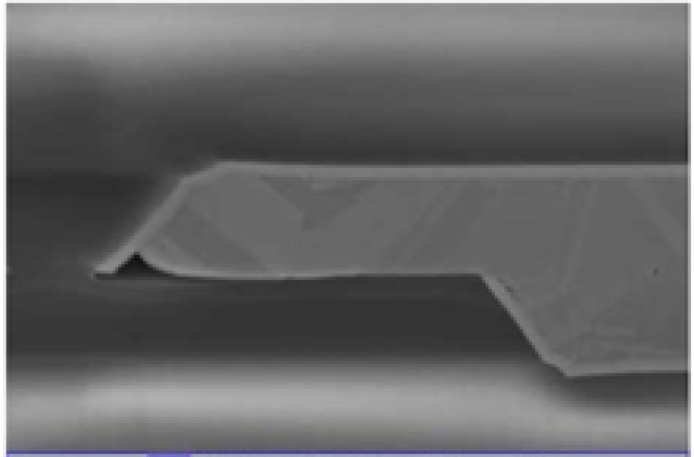
Figure 3. First demonstration of Cu/BCB hybrid bonding [16]
-
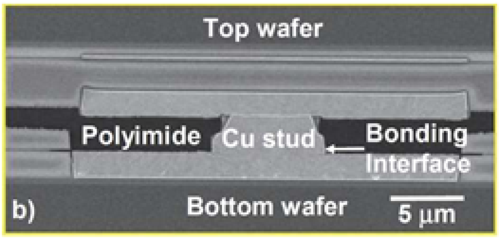
Figure 4. Demonstration of Cu/Polymer hybrid bonding using Lock-n-Key technology [18]
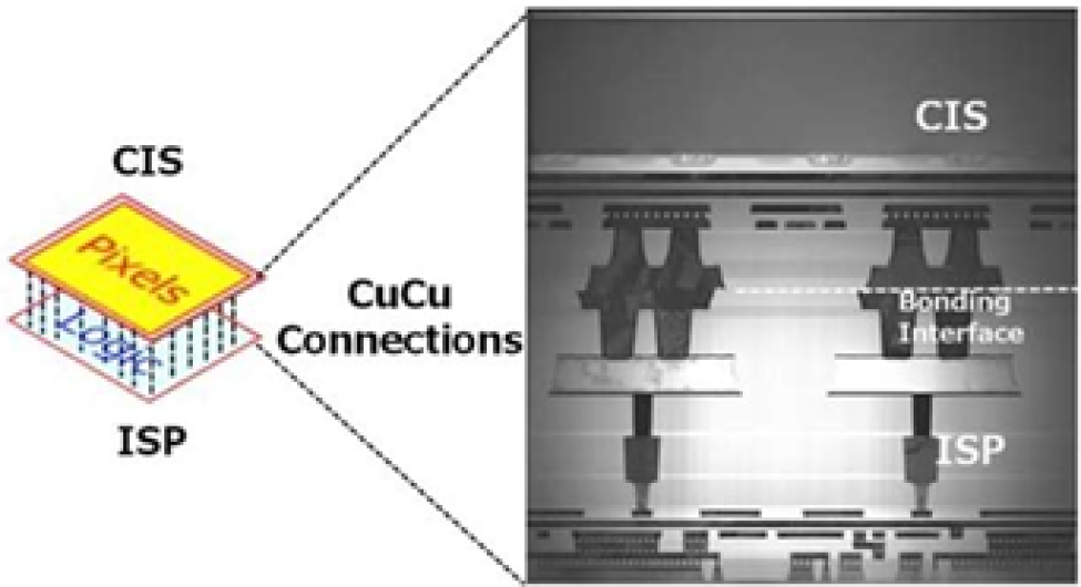
When considering thermocompression Cu/SiO₂ hybrid bonding, the ideal approach is to directly use damascene copper alongside the adjacent silicon dioxide dielectric material as the bonding medium. However, due to the nature of the damascene process, the copper surface often has depressions, with depths reaching up to 50 nm, depending on the size of the copper pads. For example, in Figure 6, the copper surface is approximately 20 nm lower than the silicon dioxide surface [21]. Even such a small depression can lead to poor surface morphology of the copper bond, as the harder silicon dioxide surface makes contact first, hindering contact at the center of the copper pad. Therefore, developing hybrid bonding based on damascene structures has become a significant challenge, a problem that was raised about 20 years ago. Interestingly, the unique characteristics of damascene copper have prompted researchers to develop another hybrid bonding technique, namely Direct Bond Interconnect (DBI). Although DBI initially did not use the term "hybrid bonding," its core concept is consistent: two wafers or chips with recessed copper pads surrounded by silicon dioxide are first bonded at room temperature through oxide-to-oxide bonding. Subsequently, during the annealing process at copper-to-copper bonding temperatures (e.g., 400°C), the thermal expansion coefficient (CTE) of copper, which is greater than that of silicon dioxide, causes the filling of the copper depressions, ultimately forming expanded contact and bonding of the copper pads, as shown in Figure 7 [22].
It is worth noting that this method does not require the application of pressure or the use of a vacuum environment for copper-to-copper bonding, giving it the potential for mass production. In addition, the bonding of oxide to oxide can be completed at room temperature, significantly reducing the process time compared to thermal compression bonding, which will also result in higher production capacity.
-
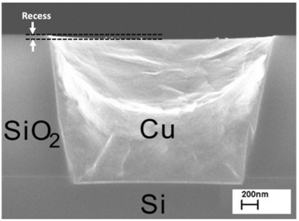
Figure 6. Cu/SiO₂ Surface Morphology
-
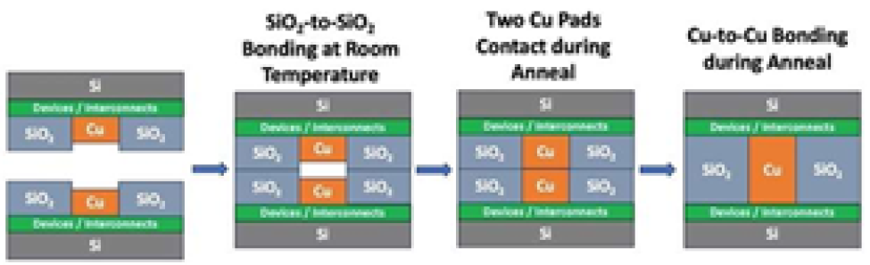
Figure 7. Schematic diagram of the hybrid bonding process based on DBI
Current technological achievements and status
Like other industry efforts, the imec research team is also actively developing hybrid bonding technology. Unlike traditional materials, imec uses silicon carbon nitride (SiCN) as the dielectric material, which is widely used in back-end-of-line (BEOL) interconnections, has an extremely low surface roughness (only 0.1 nm after CMP), and has a very high bonding energy for silicon carbon nitride. Recently, imec's E. Beyne team successfully demonstrated wafer-level hybrid bonding with a spacing of 400 nm and a copper pad size of only 200 nm, as shown in Figure 9 [23]. These results of fine-pitch hybrid bonding demonstrate the possibility of achieving high-density interconnections through three-dimensional integrated circuit integration.
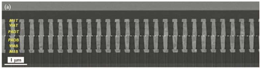
Figure 9. 400nm pitch hybrid bonding interconnection [23]
Since the bonding temperature is closely related to stress, warpage, and component performance, although a bonding temperature of 400°C meets the thermal budget of CMOS, developing bonding technology at lower temperatures remains a key issue. Copper-to-copper bonding typically requires high temperatures of 300-400°C, primarily due to the presence of an oxide layer on the copper surface, which hinders the diffusion of copper atoms from the two substrates. Therefore, sufficiently high temperatures must be provided to facilitate the diffusion of copper atoms and grain growth, thereby achieving bonding. Professor Chen Guan-neng's research team successfully demonstrated a technique for low-temperature copper-to-copper bonding using a metal passivation layer. By depositing a very thin (about 10 nm) metal passivation layer on the copper surface, copper oxidation can be effectively prevented, as shown in Figure 10 [24].
In this technology, when specific metals are used as passivation layers, during the bonding process, copper atoms tend to penetrate the grain boundaries of the thin passivation layer and reach the bonding interface. At this time, the copper atoms from the two substrates have not yet been affected by oxidation, allowing them to smoothly form a bonding structure. It is noteworthy that this phenomenon occurs only with specific metals, such as gold, silver, palladium, and titanium. Furthermore, research has shown that the diffusion pathway of copper atoms primarily occurs through the grain boundaries of the passivation layer, and the thickness and surface roughness of the passivation layer are key factors affecting the success of the bonding. In this copper-to-copper bonding platform, by appropriately controlling the thickness and surface roughness of the passivation layer, a bonding temperature close to room temperature of 40°C has been successfully achieved, and the bonding strength can be enhanced through subsequent annealing. Generally speaking, metal passivation-based copper-to-copper bonding technology has been successfully demonstrated at both wafer-to-wafer (W2W) and chip-to-wafer (C2W) scales, with bonding temperatures below 150°C. As shown in Figure 11, the Cu/SiO₂ hybrid bonding technology through the metal passivation layer not only exhibits excellent reliability but also possesses good electrical performance. In addition to achieving bonding at the lowest possible temperature, it is more important that the principle of the metal passivation layer comes from the protection of the surface metal film and does not intentionally change the grain and orientation of the copper material, thus it will not be limited by size miniaturization in applications.
-
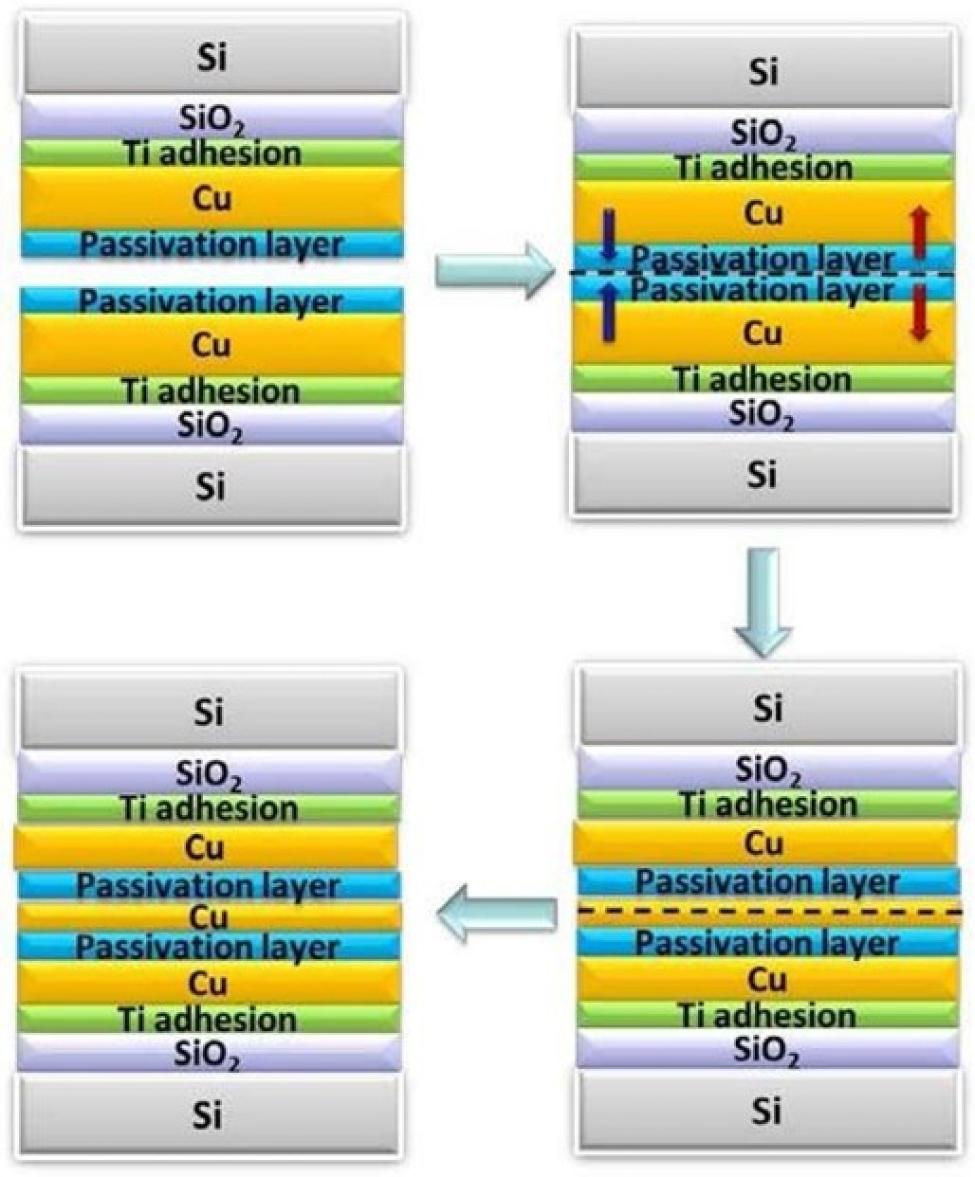
Figure 10.Metal passivation layerCu for CuBonding Schematic[24]
-
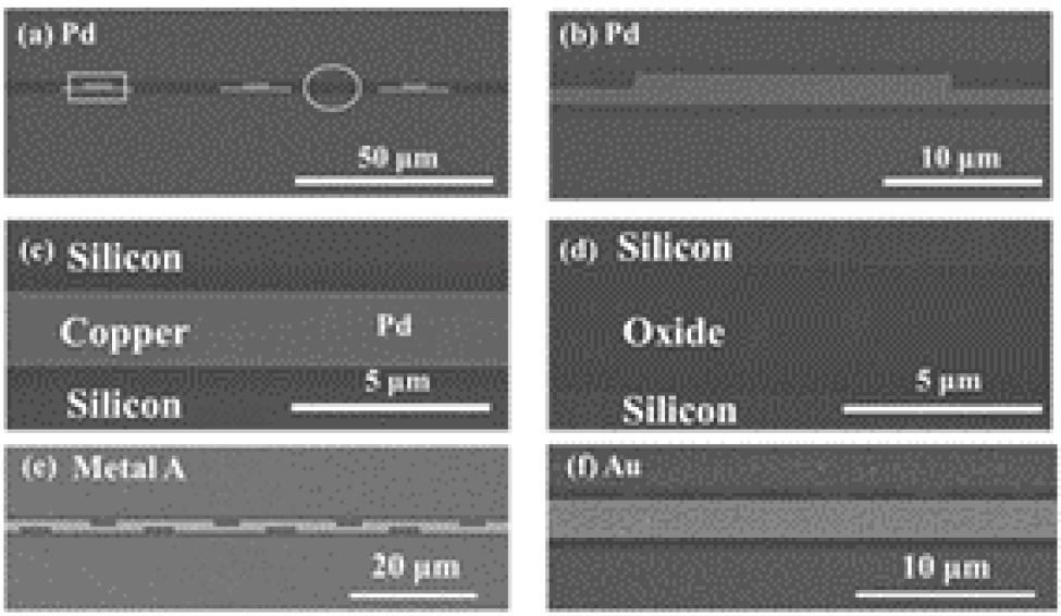
Figure 11. Cu/SiO2Hybrid bonding and various metal passivation layers[21]
Future Trends and Conclusion
Since hybrid bonding is often associated with high-performance computing (HPC) and high bandwidth memory (HBM) technology nodes, high yield and high reliability multi-chip stacks will become standard requirements. However, since stacking involves multiple thinned chips, and the hybrid bonding process is accompanied by temperature increases, significant stress and warpage will occur in the bonding system, which in turn affects subsequent processes and packaging. Therefore, developing low-temperature hybrid bonding technology is a key challenge. Additionally, selecting suitable hybrid bonding materials (especially dielectric materials) is crucial for determining the appropriate bonding methods (such as DBI or TCB). For example, SiCN has been successfully applied in hybrid bonding, and various polymer materials have also been proposed to reduce bonding temperature and processing time. Furthermore, the industry is exploring alternative materials to copper to achieve lower temperature bonding. Finally, a precise hybrid bonding device is undoubtedly a key factor in ensuring successful bonding results. In addition to requiring a highly clean bonding environment, the surface conditions and particle control during the bonding process heavily depend on the performance of the bonding device. Moreover, alignment accuracy is critical for controlling the copper pad spacing and size in hybrid bonding. In future logic and memory stacking applications, due to the increased interconnect density, sub-micron level alignment error control has become a basic requirement. Therefore, the precision and performance of hybrid bonding devices are crucial.
In the past two decades, hybrid bonding technology has made significant breakthroughs in the field of three-dimensional integrated circuits and advanced packaging. With the development of copper-to-copper bonding and DBI bonding, this technology has been widely applied in wafer-to-wafer and chip-to-wafer processes, driving continuous technological innovation. Hybrid bonding continues to push the limits of system miniaturization, performance, and efficiency. The development of key technologies such as low-temperature hybrid bonding and fine-pitch interconnects has addressed many challenges and met the stringent demands of advanced semiconductor systems. Looking ahead, material development, improvements in bonding and CMP devices, as well as new bonding methods, will play a key role in overcoming remaining challenges, such as reducing costs, improving yield, minimizing warpage, and managing multi-chip stack stress. By addressing these critical issues, hybrid bonding technology will play an important role in the development of high-density, low-power, and highly reliable semiconductor devices.
Reference:
[1] R. Reif, A. Fan, Kuan-Neng Chen, and S. Das, "Fabrication technologies for three-dimensional integrated circuits," Proceedings International Symposium on Quality Electronic Design, San Jose, CA, USA, 2002, pp. 33-37, doi: 10.1109/ISQED.2002.996687.
[2] V. Chidambaram et al., “Dielectric Materials Characterization for Hybrid Bonding,” Proc. IEEE 71st Electronic Components and Technology Conference (ECTC), 2021, pp. 426-428. DOI: 10.1109/ECTC32696.2021.00078.
[3] K. N. Chen, A. Fan, C. S. Tan, and R. Reif, "Microstructure Evolution and Abnormal Grain Growth During Copper Wafer Bonding," Applied Physics Letters, vol. 81, no. 20, pp. 3774-3776, 2002.
[4] T. Fukushima, T. Tanaka, and M. Koyanagi, "Three-Dimensional Integration Technology with Through-Silicon Vias and Microbumps," Japanese Journal of Applied Physics, vol. 47, no. 4S, pp. 2801-2808, Apr. 2008.
[5] C. S. Tan, K. N. Chen, and S. J. Koester, "Wafer-Level 3-D Integration Technology," IEEE Transactions on Electron Devices, vol. 55, no. 3, pp. 1003-1010, Mar. 2008.
[6] K. N. Chen, "Advances in Low-Temperature Cu-to-Cu Direct Bonding," IEEE Transactions on Components, Packaging and Manufacturing Technology, vol. 7, no. 4, pp. 557-567, Apr. 2017.
[7] B. Zhang, F. Niklaus, G. Stemme, and E. Beyne, "Scaling Cu/SiCN Wafer-to-Wafer Hybrid Bonding Down to 400 nm Interconnect Pitch," IEEE 74th Electronic Components and Technology Conference (ECTC), Denver, CO, USA, 2024, pp. 312-318.
[8] M. Motoyoshi, "Through-Silicon Via (TSV)," Proceedings of the IEEE, vol. 97, no. 1, pp. 43-48, Jan. 2009.
[9] E. Beyne, "3D System Integration: Hybrid Bonding and Beyond," IEEE International Electron Devices Meeting (IEDM), San Francisco, CA, USA, Dec. 2019, pp. 676-679.
[10] Kuan-Neng Chen, Andy Fan, and Rafael Reif, "Microstructure Examination of Copper Wafer Bonding," Journal of Electronic Materials, 30, pp 331- 335, 2001.
[11] K. N. Chen, A. Fan, C. S. Tan and R. Reif, “Microstructure evolution and abnormal grain growth during copper wafer bonding,” Applied Physics Letters, 81(20), pp 3774-3776, 2002.
[12] K. N. Chen, A. Fan, C. S. Tan, and R. Reif, “Temperature and Duration Effect on Microstructure Evolution during Copper Wafer Bonding”, Journal of Electronic Materials, 32(12), pp 1371-1374, 2003.
[13] K. N. Chen, C. S. Tan, A. Fan and R. Reif, "Morphology and bond strength of copper wafer bonding", Electrochemical and Solid-State Letters, 7(1), pp G14- G16, 2004.
[14] K. N. Chen, A. Fan, C. S. Tan, and R. Reif, “Contact Resistance Measurement of Bonded Copper Interconnects for Three-Dimensional Integration Technology”, IEEE Electron Devices Letters, 25(1), pp 10-12, 2004.
[15] Kuan-Neng Chen, Sang Hwui Lee, Paul S. Andry, Cornelia K. Tsang, Anna W. Topol, Yu-Ming Lin, JianQiang Lu, Albert M. Young, Meikei Ieong, and Wilfried Haensch, "Structure Design and Process Control for Cu Bonded Interconnects in 3D Integrated Circuits", 2006 International Electron Devices Meeting (IEDM), pp. 367-370, San Francisco CA, Dec. 11-13, 2006.
[16] J. J. McMahon, J.-Q. Lu and R. J. Gutmann, "Wafer bonding of damascene-patterned metal/adhesive redistribution layers for via-first three-dimensional (3D) interconnect," Proceedings Electronic Components and Technology, 2005. ECTC '05., Lake Buena Vista, FL, USA, 2005, pp. 331-336 Vol. 1, doi: 10.1109/ECTC.2005.1441287.
[17] R.J. Gutmann, J.J. McMahon, S. Rao, F. Niklaus, and J.- Q. Lu, “Wafer-Level Via-First 3D Integration with Hybrid-Bonding of Cu/BCB Redistribution Layers”, Proceedings of International Wafer-Level Packaging Congress (IWLPC), pp. 122-127, SMTA, Nov. 2-4, 2005.
[18] R. R. Yu, F. Liu, R. J. Polastre, K.-N. Chen, X. H. Liu, L. Shi, E. D. Perfecto, N. R. Klymko, M. S. Chace, T. M. Shaw, D. Dimilia, E. R. Kinser, A. M. Young, S. Purushothaman, S. J. Koester and W. Haensch, “Reliability of a 300-mm-compatible 3DI technology based on hybrid Cu-adhesive wafer bonding”, 2009 Symposia on VLSI Technology and Circuits, Kyoto, Japan, Jun. 15-18, 2009.
[19] K. N. Chen, T. M. Shaw, C. Cabral, Jr., and G. Zuo, “Reliability and structural design of a wafer-level 3D integration scheme with W TSVs based on Cu-oxide hybrid wafer bonding”, 2010 International Electron Devices Meeting (IEDM), San Francisco CA, Dec. 6-8, 2010.
[20] Kuan-Neng Chen, Zheng Xu, and Jiang-Qiang Lu, "Electrical Performance and Alignment Investigation of Wafer-level Cu-oxide Hybrid Bonding," IEEE Electron Device Letters, 32(8), pp. 1119-1121, Aug 2011.
[21] K.N. Chen, C.K. Tsang, A.W. Topol, S.H. Lee, B.K. Furman, D.L. Rath, J.-Q. Lu, A.M. Young, S. Purushothaman, and W. Haensch, "Improved Manufacturability of Cu Bond Pads and Implementation of Seal Design in 3D Integrated Circuits and Packages", 23rd International VLSI Multilevel Interconnection (VMIC) Conference, Fremont CA, Sep.25-28, 2006.
[22] Y. Kagawa et al., "An Advanced CuCu Hybrid Bonding For Novel Stacked CMOS Image Sensor," 2018 IEEE 2nd Electron Devices Technology and Manufacturing Conference (EDTM), Kobe, Japan, 2018, pp. 65-67, doi: 10.1109/EDTM.2018.8421453.
[23] B. Zhang et al., "Scaling Cu/SiCN Wafer-to-Wafer Hybrid Bonding down to 400 nm interconnect pitch," 2024 IEEE 74th Electronic Components and Technology Conference (ECTC), Denver, CO, USA, 2024, pp. 312- 318, doi: 10.1109/ECTC51529.2024.00058.
[24] Yan-Pin Huang, Yu-San Chien, Ruoh-Ning Tzeng, and Kuan-Neng Chen, "Demonstration and Electrical Performance of Cu–Cu Bonding at 150 °C With Pd Passivation," IEEE Transactions on Electron Devices, 62(8), pp. 2587-2592, Aug. 2015.
[25] Zhong-Jie Hong, Demin Liu, Shu-Ting Hsieh, Han-Wen Hu, Ming-Wei Weng, Chih-I Cho, Jui-Han Liu, and Kuan-Neng Chen, "Room Temperature Cu-Cu Direct Bonding Using Wetting/Passivation Scheme for 3D Integration and Packaging," 2022 Symposia on VLSI Technology and Circuits, Honolulu, HI, Jun. 12-17, 2022.
[26] Demin Liu, Po-Chi Chen, Chien-Kang Hsiung, Shin-Yi Huang, Yan-Pin Huang, Steven Verhaverbeke, Glen Mori, and Kuan-Neng Chen, “Low Temperature Cu/SiO2 Hybrid Bonding with Metal Passivation,” 2020 Symposia on VLSI Technology and Circuits, Virtual Conference, Jun. 14-19, 2020.


