
K-kit - An innovative microchip for in-situ electron microscopy analysis of nano solutions.
K-kit - An innovative microfluidic chip for in-situ electron microscopy analysis of nanofluids.
The K-kit Innovative Microchip for in-situ Electron Microscopy of Nanofluids
Chen Hung-Jen
Hung-Jen Chen
-
With the expansion of applications for nanofluids, global detection standards for liquid-phase nanoproducts are becoming increasingly stringent, requiring precise analysis of nanoparticle morphology and distribution in solutions. In recent years, transmission electron microscopy (TEM) has made progress in liquid-phase in-situ analysis, particularly with microfluidic chip technology. This article introduces an innovative microfluidic chip "K-kit," which utilizes capillary forces for rapid solution loading, is compatible with various TEM equipment, and enhances nanoparticle image contrast through wet negative staining. K-kit has several unique product advantages and has been widely adopted in academic research and industries such as electronics, chemicals, pharmaceuticals, and food for nanofluid analysis.
With the expanding applications of nanofluids, global standards for the analysis of liquid-phase nanoproducts are becoming increasingly stringent, requiring precise characterization of nanoparticle morphology and distribution in solution. In recent years, transmission electron microscopy (TEM) has made significant advancements in in-situ liquid analysis, particularly with the development of microfluidic silicon chip technology. This article introduces an innovative microfluidic chip, "K-kit," which uses capillary forces to quickly load the solution, is compatible with various brands of TEM equipment, and enhances nanoparticle image contrast through wet negative staining. K-kit offers several unique advantages and has been widely applied in academic research as well as industries such as electronics, chemical engineering, pharmaceuticals, and food etc.
1. The analysis needs and challenges of nanofluids
The application of nanofluids has penetrated daily life. With the development of nanotechnology, countries in Europe and America have recently begun to promote labeling and review regulations for liquid nanoproducts, emphasizing the need for comprehensive analysis of the physicochemical properties of the final products. Particularly in liquid environments, it is crucial to evaluate key characteristics of newly added nanomaterials, such as component types, size and shape, particle concentration, particle size distribution, and aggregation, to ensure the safety and stability of the products.
In May 2012, the International Organization for Standardization (ISO) released ISO/TR 13014:2012 "Nanotechnologies - Guidance on Physico-chemical Characterization of Engineered Nanoscale Materials for Toxicologic Assessment," emphasizing that a physico-chemical characterization must be completed before conducting toxicological assessments to establish the correlation between nanomaterials and test results. As shown in Figure 1, the standard lists eight key parameters for nanomaterial testing. These parameters are crucial for assessing the safety, environmental impact, and product applications of nanomaterials. Additionally, ISO/TR 13014:2012 provides a set of standardized testing methods to help research institutions and companies establish a consistent evaluation process for nanomaterials.
__26D16kT4YC.jpg "1 (2)")
Figure 1. Eight important nano-detection parameters of ISO/TR13014 standard (2012 edition)
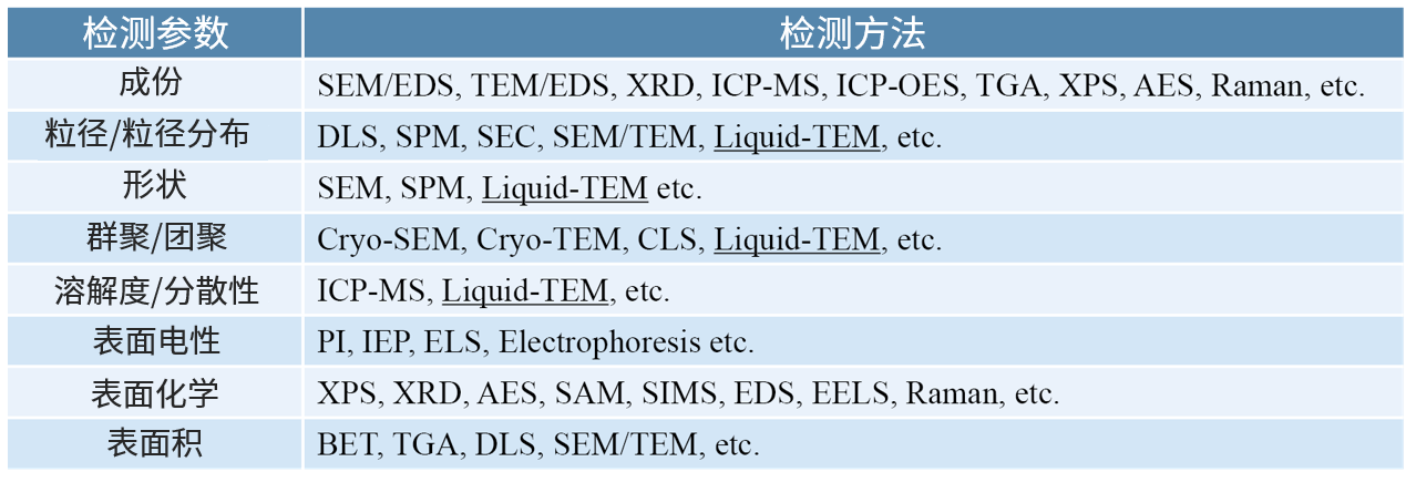
The analysis methods for nanomaterials are listed in Table 1. Most projects can now be tested using commercially available instruments, but the analysis technology for nanofluids still faces many challenges. In particular, for the four detection parameters of "shape," "particle size/size distribution," "aggregation/ agglomeration," and "solubility/dispersibility," it is necessary to obtain actual imaging information of the particles in the solution to ensure the accuracy of the analysis results. To meet the testing needs of the nanotechnology industry, directly observing nanoparticles in solution using electron microscopy at the microscopic scale would help obtain the most authentic imaging information about product composition and characteristics.
Table 1. Common Analysis Methods for Nanomaterials
Transmission electron microscopy has long been a key technology for exploring material structures. In recent decades, this technology has undergone several breakthrough developments, such as aberration correction technology achieving atomic-scale imaging, Cryo-TEM technology providing high-resolution imaging of biological samples, and various innovative TEM structural designs enabling in-situ analysis of dynamic systems. In recent years, in-situ techniques based on silicon chip application architectures have rapidly developed, allowing experiments to observe dynamic changes in materials and biological samples under simulated real environmental conditions, all within the high vacuum environment of the TEM chamber. Among them, one of the most notable technologies is the use of silicon chips to encapsulate liquids, enabling nanoscale liquid-phase dynamics observations within the TEM.(1)Through in-situ liquid TEM imaging to observe liquid-phase reactions, researchers can delve into the fundamental principles of important fields such as electrochemical processes, antibacterial and pathological mechanisms, and biological cell behavior.
2. Evolution of Liquid-phase In-situ Electron Microscopy Technology
The development of in-situ electron microscopy technology has broken through the limitations of traditional electron microscopy, which could only be performed in a high vacuum environment. As early as the 1950s to 1960s, scholars began to explore electron microscopy observations in controlled gas environments and found that these gas environment techniques effectively reduced the damage of the electron beam to the samples. Among them, Heide (1962)(2)The related research laid an important foundation for subsequent electron microscopy observations in liquid environments. However, directly modifying the device structure and constructing fluid pipelines within the TEM vacuum chamber not only incurs high costs and poses challenges for cleaning and maintenance, but also carries the risk of solution leakage. Additionally, due to the limitations of traditional machining precision, it is also difficult to obtain high-resolution nanoparticle images (with thicker liquid layers).
In the 1990s, the technology of liquid cells (liquid cell, LC) was introduced. This technology uses robust thin film materials (such as silicon nitride SiN) to encapsulate solution samples, allowing them to remain in liquid form in electron microscopes without affecting the penetration of the electron beam. With advancements in precision processing technology, dynamic observation capabilities and more powerful liquid flow cells (liquid flow cell, LFC) gradually developed. The core of this technology lies in the use of specially designed TEM sample holders (TEM holder), which integrate a flow channel system internally. At the front end of the sample holder, two silicon wafers, a metal cover plate, and sealing rings are precisely locked together to form a liquid cell observation window with liquid flow capabilities, enabling researchers to observe dynamic changes in nanoscale liquid samples. Currently, Oak Ridge National Laboratory (ORNL) and the National Center for Electron Microscopy (NCEM) are at the forefront of this research field and actively support several commercial design companies for in-situ TEM holders, such as Hummingbird Scientific.(17)and Protochips(18)to promote the development and sales of actual products. In addition, companies such as DENSsolutions from the Netherlands and Nanofactory from Sweden have also entered the market, becoming important competitors in the field.
Due to the advancements in semiconductor processes and precision machining technology, current in-situ liquid TEM holder products can support functions such as liquid flow, heating, and electrical conduction. Researchers can manipulate the liquid environment within the electron microscope to achieve continuous reaction observations, thereby promoting research in areas such as nanomaterial growth, catalytic reactions, and electrochemical reactions. Figure 2 shows the in-situ liquid TEM holder products and accessories launched by Protochips. However, such in-situ observation technologies typically rely on sample holders provided by specific manufacturers and must be used with specially designed silicon chips, resulting in limited device compatibility and high costs. Additionally, the processes of assembling the sample holder, leak testing, pre-treatment, and cleaning are quite cumbersome, often requiring several hours for a single observation. Therefore, the current applications of in-situ liquid TEM holder products are mainly concentrated in academic research, making it difficult to meet the industry's demand for efficient, low-cost, and large-scale sample analysis.
__26D16XcnvQ.jpg "3(1)") Figure 2. The liquid in-situ TEM sample rod product from Protochips, USA (Image source: (18))
Figure 2. The liquid in-situ TEM sample rod product from Protochips, USA (Image source: (18))
In 2016, the well-known domestic semiconductor testing company MA-tek (Materials Analysis Technology Inc.) developed the monolithic microfluidic chip "K-kit" based on its exclusive patented technology, bringing innovative breakthroughs to the TEM image analysis of nanofluid samples.(16)As shown in Figure 3, the K-kit uses a standard 3 mm diameter TEM copper ring as the carrier platform, which has high compatibility and can be directly applied to electron microscope devices from major brands such as Hitachi, FEI, and JEOL, without the need to purchase expensive liquid in-situ TEM sample rods. In addition, its monolithic structure design greatly simplifies the sample preparation process, making operations faster and more convenient, while also reducing testing costs. Figure 4 shows the electron microscopy imaging results of K-kit for different nano solutions. With its high applicability, convenience, and cost-effectiveness, the K-kit not only meets the analytical needs of academic research but also provides practical detection solutions for liquid nano materials in the industry.
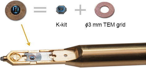
Figure 3. The K-kit uses a standard copper ring for TEM support, making it suitable for observation with various brands of TEM equipment.
__26D16iKqJY.png "5(1)")
Figure 4. Electron microscopy imaging results of K-kit for various types of nanofluid samples.
3. The New Tool for Nanofluid Analysis: K-kit
3.1 K-kit Structural Principle
The K-kit chip is made using micro electro mechanical systems (MEMS) technology, with its structure formed by aligning two symmetrically designed silicon chips through high-temperature bonding and wet etching processes. Figure 5 shows the appearance of the completed K-kit wafer and a scanning electron microscope (SEM) image of a single K-kit chip. As shown in Figure 6, there is a micro liquid storage channel located in the center of the K-kit, which allows for loading and sealing the solution through openings at both ends of the channel. The upper and lower surfaces of the K-kit body structure each have a groove, with the bottom of the groove featuring a layer of silicon nitride (Si) of nanometer thickness.3N4The liquid pool observation window composed of a thin film allows the electron beam of the electron microscope to penetrate and image. The main structure of the K-kit is made of hard silicon crystal material, and the silicon nitride thin film also has high toughness, which enables the K-kit chip to withstand significant vacuum environment pressure changes. It can also be paired with a TEM sample rod equipped with heating or cooling functions for in-situ observation of liquid samples under varying temperature conditions (recommended operating temperature range is –196 °C to 120 °C).
__26D16mxUUh.png "6(1)")
Figure 5. Structure appearance of K-kit wafer and single K-kit chip.
__26D16B1niL.png "7(1)")
Figure 6. Structure of the K-kit chip (Image source: (16))
The K-kit is a liquid-phase in-situ electron microscopy imaging analysis product that has been on the market for many years and can be purchased through over 20 well-known electron microscope consumable distributors worldwide. As shown in Figure 7, the size of the K-kit chip is 1.7mm × 1.4mm × 0.8mm, and the observation window size in the grooves on the upper and lower surfaces is 300μm × 25μm. The opening size of the microchannels at both ends of the main structure determines the size of the nanoparticles that can be loaded. Therefore, to meet the observation needs of different samples, the K-kit product offers six channel height options: 0.1μm, 0.2μm, 0.5μm, 1μm, 2μm, and 5μm. In addition, the thickness of the silicon nitride film in the observation window also provides two options: 30 nm and 100 nm.
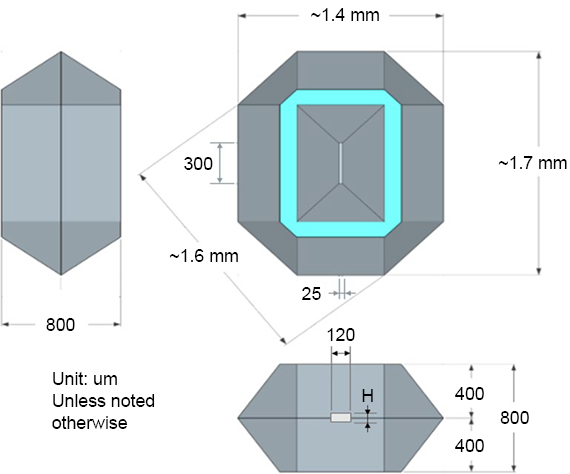
Figure 7. K-kit chip size
As shown in Figure 8, in order to facilitate the sample preparation operation of the K-kit chip, MA-tek has also designed a dedicated K-kit tool box to improve the speed and reliability of user sample preparation. Currently, there are two types of shipping packaging boxes for the K-kit, namely a four-pack and a six-pack. In addition, each K-kit is equipped with a carrier upon shipment and sealed with a transparent plastic cover for protection. The bottom of the carrier has a pre-installed TEM standard copper ring, which can be removed for use after the bottom plate is taken off.
__26D16ZPKeE.png "9(1)")
Figure 8. K-kit toolbox and shipping packaging
3.2 Sample Preparation Process
The sample preparation method for the K-kit is very simple, as shown in Figure 9. Typically, the new K-kit has a sealing block at each end to maintain a vacuum state within the microchannel, ensuring that its inner surface is highly clean to enhance the solution loading effect. When in use, the sealing blocks should first be removed using tweezers or a channel opener, and then one end of the microchannel should be gently touched to the surface of the droplet, allowing the nanofluid to be drawn into the microchannel through capillary action. After the solution is loaded, adhesive sealing at both ends and the attachment of a copper ring should follow. Once the adhesive has cured (it is recommended to place it in a simple vacuum device to accelerate drying), the K-kit sample can be loaded onto the TEM sample holder for observation. The entire sample preparation process can be completed in about 30 minutes.
__26D16Xg0iY.png "10(1)")
Figure 9. Sample preparation steps of K-kit
The monolithic structure design of the K-kit chip demonstrates unique advantages compared to in-situ liquid-phase TEM sample rods. With its integrated design, the K-kit can adapt to the solution loading amount without the need for special control of the sample droplet size. In addition, the extremely small liquid storage channels inside the K-kit can generate strong capillary forces, allowing even high-viscosity or oily samples to be directly loaded without additional dilution (tests have shown that solutions with a viscosity coefficient exceeding 3,000 mPa·s can also be successfully loaded). This design ensures the stability and reliability of solution loading and greatly enhances operational convenience.
For sealing the microchannel openings, it is recommended to use the well-known brand Torr-seal vacuum adhesive. Torr-Seal is an epoxy-based vacuum sealing adhesive with excellent sealing performance, which does not release volatile substances after curing, making it suitable for high vacuum environments. Furthermore, the material has high stability and does not react with most chemical solutions, so when sealing, even if it comes into contact with the sample solution inside the K-kit, it is not likely to cause contamination, ensuring the reliability of experimental observation results.
The K-kit body structure is made of acid and alkali resistant silicon crystal material, paired with Torr Seal adhesive, which has high stability against most chemical solutions. Therefore, it can be widely applied for the observation and analysis of various common chemical solutions. Table 2 presents the FTIR detection analysis conducted after soaking Torr Seal adhesive in various chemical solutions for 24 hours (to determine if any components dissolved) and the visual observation results (to assess whether the adhesive diffused in the solution). After long-term soaking tests, no dissolution or dispersion of Torr Seal adhesive was found in most solutions. Only a few solutions showed trace amounts of the adhesive components in the FTIR detection results. However, even so, Torr Seal demonstrated good tolerance to these specific solutions, allowing it to be used for sealing operations of the K-kit in a short period (within a few hours) and successfully completing image observation.
Table 2. Test results of Torr Seal adhesive soaked in various chemical solutions (16)
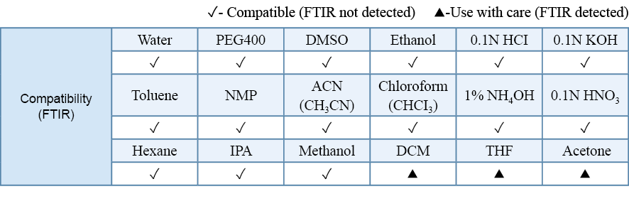
In practical applications, as long as the sample solution does not chemically react with Torr Seal, the K-kit can be used for imaging observation. According to empirical experience, even strong acids (such as sulfuric acid with a pH of about 1) or strong bases (such as ammonia with a pH of about 12) can be stably encapsulated in the K-kit for observation. However, during the preparation process of samples containing strong acids or strong bases, special attention must still be paid to operational risks, and appropriate personal protective equipment must be worn to ensure the safety of the users.
In addition, to improve the sample preparation efficiency of the K-kit and to avoid detachment during the gripping process due to poor adhesion between the copper ring and the chip, MA-tek has developed a convenient K-kit folding grid using patented technology, as shown in Figure 10. This copper grid is manufactured using MEMS technology and features a foldable design that allows for precise alignment of the upper and lower halves. Each half has a groove in the center to secure the K-kit chip, and the bottom of the groove is designed with a central opening, allowing the TEM electron beam to penetrate when the upper and lower structures are combined, enabling imaging observation.
Originally, the sample preparation of the K-kit required fixing it onto the TEM copper grid with adhesive. This method not only takes a longer time for the adhesive to cure, but also poses a risk that if the adhesive application is not careful, it may flow into the K-kit window and contaminate the silicon nitride film. By importing this specialized copper grid, it can significantly enhance the usability and sample preparation speed of the K-kit, while effectively avoiding the risk of sample preparation failure caused by improper adhesive application. Moreover, this copper grid can be reused multiple times, providing significant cost benefits.
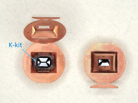
Figure 10. Appearance of the K-kit openable copper mesh
3.3 Wet and Dry Sample Preparation
The K-kit adopts a monolithic structure design, demonstrating significant differentiated characteristics in sample preparation. As shown in Figure 11, through appropriate sample preparation methods, two different liquid states, dry and wet, can be formed in the K-kit microchannel. Regardless of the dry or wet state, a uniform and consistent distribution of nanoparticles can be maintained, ensuring stable and high-quality observation results.
__26D16qzUAt.png "12(1)")
Figure 11. TEM image observation results of wet and dry K-kit. In this case, the sample loaded in the K-kit is NIST 100 nm polystyrene.
In the K-kit sample preparation process, by selecting appropriate microchannel sizes and controlling the time interval between loading the solution and sealing with adhesive, four different liquid storage state samples can be formed as shown in Table 3. Generally, it is recommended to use a K-kit with a larger channel height (e.g., 2 μm) for preparing dry samples, while a K-kit with a smaller channel height (e.g., 0.2 μm) is more suitable for preparing wet samples. The main reason is that the K-kit with a larger channel height has a larger opening, making it easier for the liquid to naturally evaporate at room temperature or to be quickly removed in a vacuum environment. Therefore, when preparing dry samples, there is no need to coat vacuum adhesive at both ends of the channel for sealing, ensuring that the solution is completely dried.
Table 3. Different liquid sample preparations achievable with the K-kit.
__26D166yamJ.png "13(1)")
Users can choose to prepare dry or wet K-kit samples based on their analysis needs. If the goal is only to observe the morphology, size, or aggregation state of particles in the solution, it is recommended to prioritize the dry K-kit for better TEM image quality. If the research objective involves chemical reactions in the solution (for example, the gold reduction reaction of AuCl4– solution under electron beam), or if it is necessary to maintain the solution within the K-kit (such as observing the true morphology of biological or organic particles), then the wet K-kit is suitable. Additionally, some sample solutions may easily produce bubbles or disturbances under TEM electron beam irradiation, which can affect the clarity and stability of image observation; in such cases, the dry K-kit preparation method can be used to improve this by reducing the amount of solution in the channel, thereby minimizing the electron beam's impact on the sample. The preparation of dry mode K-kit samples allows for complete drying within the channel or the formation of a thin liquid layer of nanometer thickness on the wall, effectively enhancing image observation quality. This is also one of the main advantages of K-kit compared to other liquid cell chip products on the market.
3.4 Wet Negative Staining and Multiple Loading
Based on its unique monolithic structure, the K-kit is also the only microfluidic chip on the market that can achieve multiple loadings and wet negative staining applications. This advantage provides significant assistance for observing biological samples with low image contrast or for research in immunoelectron microscopy.
The K-kit can be applied in experimental studies that require multiple loadings of different sample solutions, such as research on catalytic reaction mechanisms or the development of immunoassay techniques, as shown in Figure 12. This unique feature is not achievable with other types of products on the market, such as two-piece combination liquid cell chips or in-situ liquid TEM sample holders.
__26D16FpeXP.png "14(1)")
Figure 12. Multiple sample loading operations can be performed using the K-kit, and there is no limit to the number of reloads.
Figure 13 is a research case of K-kit applied in immunodetection.(5)In this example, the α particles of platelets that have undergone separation treatment were repeatedly loaded through the K-kit, successfully obtaining clear TEM images of the nanoparticle gold-labeled α particles (α Granules). The preparation process of the immunological sample using the K-kit is as follows: first, different solutions were loaded through the K-kit for internal cleaning and surface treatment, then the primary antibody Mouse monoclonal anti-P-selectin antibody and the secondary antibody 6-nm gold-conjugated goat anti-mouse IgG antibody were sequentially loaded, and cultured in an environment heated to 37 °C for about 2 hours to allow the antibodies to react. Since the electron microscope cannot detect fluorescence signals, this immunogold labeling method clearly marks the position of all α particles released by platelets by combining gold particles with antibodies, utilizing the high contrast of gold in electron microscope images.
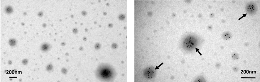
Figure 13. Using the K-kit and multiple loading steps, the TEM image results of 6 nm gold nanoparticles labeling platelet release α particles were successfully obtained. (Image source: (5))
For biological samples with lower contrast, such as viruses, bacteria, liposomes, or exosomes, a commonly used image enhancement method for electron microscopy observation is the so-called negative staining treatment. The principle of negative staining is to accumulate heavy metal dye around the nano samples, thereby deepening the image background and further highlighting the morphology of the sample. The traditional negative staining method involves adding the dye onto a copper grid with the sample placed on it, allowing it to dry, and then loading the copper grid into the electron microscope for observation. However, during this drying process, organic samples often experience structural collapse due to moisture loss, especially for vesicular biological samples such as liposomes or exosomes, which can easily lead to the collapse of the sample particles that should appear spherical and the accumulation of dye. MA-tek, based on its rich experience in biomedical sample analysis, has developed a unique K-kit wet negative staining technology that can achieve the sample negative staining effect in a "wet" solution state, successfully enabling clear electron microscopy observation of low-contrast biological samples in a liquid environment.
The K-kit wet negative staining method is very simple. Typically, a 2% uranyl acetate (UA) solution can be used as a negative stain. After uniformly mixing 10μL of the sample solution with 10μL of the negative stain, it can be directly loaded into the K-kit for observation. Users are advised to appropriately adjust the mixing ratio of the negative stain and sample solution based on actual test results to achieve the best negative staining effect. Figure 14 shows the negative staining observation results of artificial collagen fiber bundles on copper grids and K-kit. As shown in Figure 14(b), after wet negative staining treatment with the K-kit, the bundled structure image of the collagen sample can be clearly observed in the solution state. Figure 15 shows two types of biological samples with extremely low image contrast: microvesicles and exosomes.(5)the K-kit imaging observation results after its negative staining treatment.
__26D167QDbR.png "16(1)")
Figure 14. Negative staining images of collagen fiber bundles on copper grids and K-kit.
__26D16Tsyjx.png "17(1)")
Figure 15. Observation results of K-kit wet negative staining for biological samples with low image contrast.
3.5 Other Product Features
The K-kit is not only applicable for observation with various brands of TEM devices, but it is also the only microfluidic chip product on the market that can be used simultaneously for scanning electron microscopy and focused ion beam-scanning electron microscopy (FIB-SEM) observations. Figure 16 shows a comparison of images of 100 nm NIST polystyrene particles observed in a liquid environment using TEM and FIB-SEM.
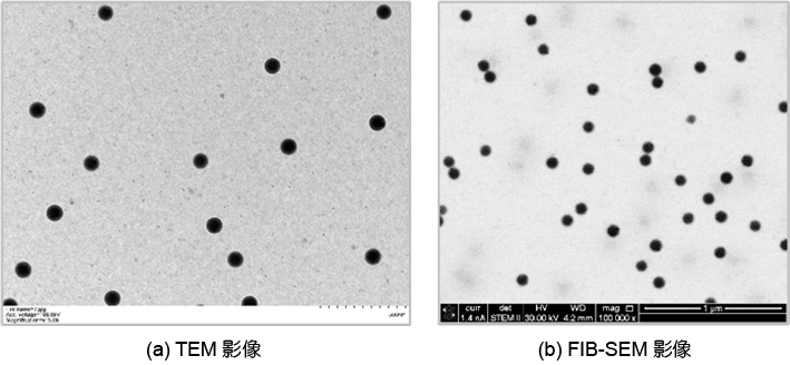
Figure 16. Comparison results of K-kit images observing 100nm polystyrene particles using TEM and FIB-SEM (The observation devices used in this case are Hitachi HT7700 TEM and FEI Helios 400 FIB)
In addition, the observation window of the K-kit is composed of an ultra-thin (approximately 30nm) silicon nitride film, which not only allows for electron beam penetration imaging in electron microscopy but also enables analyses of nanoparticles, including energy-dispersive X-ray spectroscopy (EDX) composition and lattice diffraction. Figure 17 shows the image of gold particles formed after the electron beam reduction reaction of the chloroauric acid (AuCl4) solution loaded into the K-kit via FIB-SEM observation, along with the corresponding EDX elemental analysis results. Figure 18 presents the TEM lattice diffraction pattern observation results of the nanoparticle samples within the K-kit.
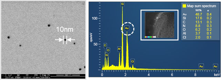 Figure 17. Observation of gold particle images in the K-kit using FEI Helios 400 FIB-SEM and its EDX analysis results (Image source:(16))
__26D16Efq6z.png "20(1)")
Figure 18. TEM lattice diffraction analysis results of nano gold particles in K-kit (Image source: (16))
3.6 K-kit Application Examples
The K-kit demonstrates high application potential in the electron microscopy observation of liquid samples, supporting analytical needs across multiple fields. For example, in the electronics industry, it can be applied to the development and process control of liquid nanomaterials; in the biomedical field, it is suitable for new drug development and research on pathological mechanisms; in the food and beverage industry, it can be used to analyze the composition and distribution of additives in products. Additionally, the K-kit can also be applied to beauty products, testing items such as sunscreen or toners containing nanomaterials.(6, 13)providing an efficient and accurate comprehensive nano-solution testing solution. Figure 19 application case is to directly load the chemical mechanical polishing solution (CMP Slurry) used in semiconductor processes into the K-kit for TEM imaging observation and particle size distribution quantitative analysis. Figure 20 is an actual example of analyzing the newly added titanium dioxide (TiO2) nanoparticles in commercial sunscreen products.
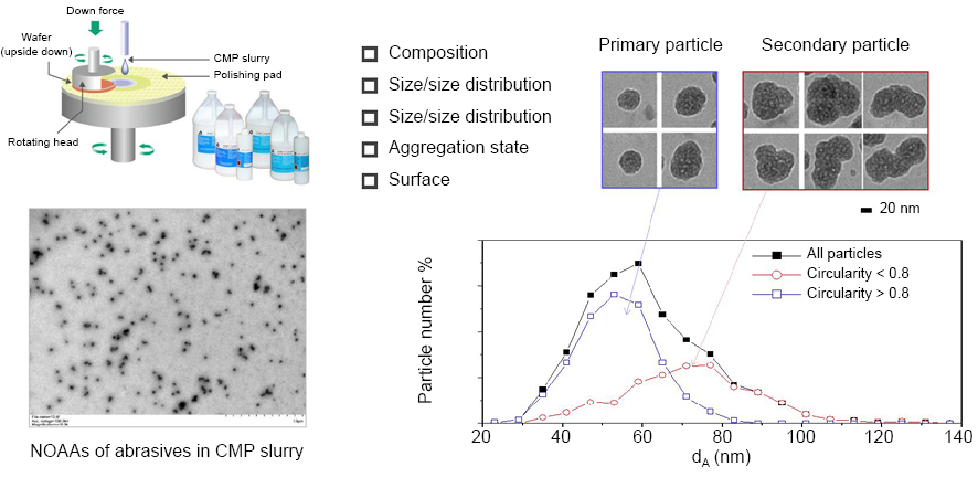 Figure 19. Results of K-kit loading CMP solution for TEM image analysis.
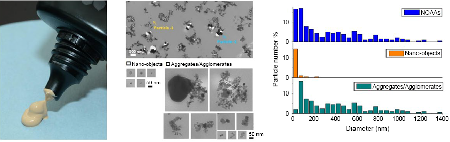
Figure 20. K-kit image analysis results of commercial sunscreen products with added TiO2 nanoparticles.
Especially in the field of nano-medicine, the K-kit also demonstrates outstanding application value. It can be used in new drug development, biomedical research, disease detection, blood screening, etc., providing concrete and intuitive electron microscopy images of liquid samples, aiding the development of medical diagnosis and scientific research. Figure 21 is a practical case of using the K-kit to analyze the size distribution of protein particles in Abraxane® drug solution.
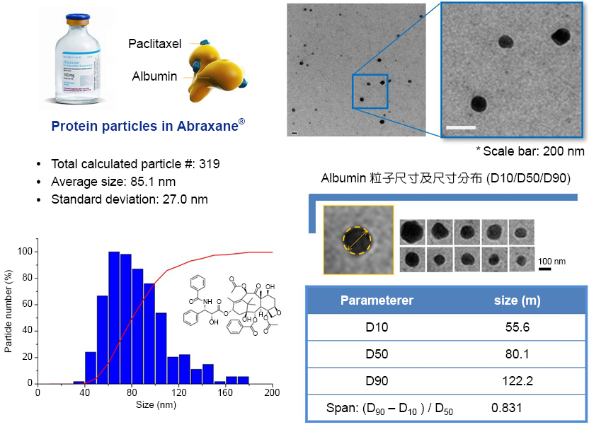 Figure 21. Analysis of protein particle image distribution in Abraxane® drug solution using K-kit.
As early as 2008, research teams were the first to use the K-kit to achieve electron microscopy imaging observations of live cells in a liquid phase environment.(7)The study successfully observed live Escherichia coli cells using the K-kit, as shown in Figure 22, as well as the process of selenite reduction by Klebsiella pneumoniae. In addition, the research also showed that Klebsiella pneumoniae and Saccharomyces cerevisiae in the K-kit could survive for up to 14 seconds and 42 seconds, respectively, under continuous TEM observation. This experimental study not only significantly simplified the liquid-phase TEM sample preparation process but also achieved the earliest results in live cell electron microscopy imaging research. Although the technology still has limitations in resolution and free radical protection, its innovative application is still regarded as an important milestone in the field of liquid-phase biological imaging.(10)。
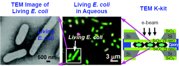 Figure 22. Successful observation of live Escherichia coli cells using K-kit (Image source: (7))
In addition, through the application of the liquid pool chip K-kit, a complete physicochemical analysis of the nanoparticles contained in blood samples in the original liquid environment, either "in vitro" or "in vivo," can be conducted. This demonstrates a high application potential in areas such as drug absorption, distribution, metabolism, and excretion (pharmacokinetics) research, as well as substance toxicity assessment. In 2012, scholars conducted related experimental research using the K-kit.(8)It will mix gold nanoparticles modified with different polymers such as citrate and polyethylene glycol (PEG) with blood, and load them into the K-kit to observe the dispersion of the gold particles. At the same time, this study will inject cPEG5k modified gold nanoparticles into mice to track the changes in their concentration in the blood over time, and compare the results with the data obtained from inductively coupled plasma mass spectrometry (ICP-MS). As shown in Figure 23, the imaging results from the K-kit are highly consistent with the trend of gold particle concentration changes measured by ICP-MS, indicating that the K-kit has practical application potential for both qualitative and quantitative analysis.
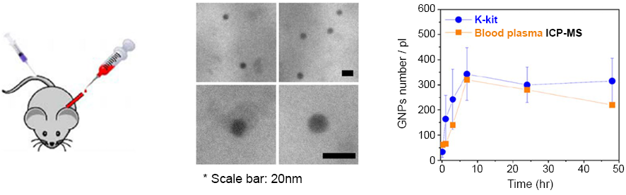 Figure 23. Injecting PEG-modified gold nanoparticles into mice, and analyzing the trend of gold particle concentration in the blood over time using K-kit and ICP-MS, and comparing the analysis results of the two methods (Image source: (8))
In 2022, scholars used the K-kit to observe for the first time the dynamic development process of Acetobacter aceti in the decomposition of glutathione.(9)As shown in Figure 24, this study clearly observed the four major stages of glutathione decomposition of acetic acid bacteria through the K-kit, including attachment and internalization, early destruction, significant destruction, and complete destruction, demonstrating the application potential of the K-kit in microbial dynamic research.
__26D16v7nlU.png "26(1)")
Figure 24. Observation of the complete destruction process of A. aceti bacteria treated with glutathione-modified gold nanoclusters (GSH-AuNC) using the K-kit (scale bar: 2μm). The imaging times for this example are: (a) 80 minutes, (b) 86 minutes, (c) 96 minutes, and (d) 114 minutes after co-culturing GSH-AuNCs with A. aceti. (Image source:(9))
In 2024, the research team successfully developed a rapid electron tomography technique by combining the K-kit liquid pool chip application, achieving an innovative method for quantitative three-dimensional (3D) structural analysis of small colloidal assemblies containing nano gold particles in an in-situ liquid phase environment.(11)Colloidal assemblies are ordered or disordered structures formed by nano- or micro-scale colloidal particles through self-assembly, self-aggregation, or external force manipulation. These structures have high designability and multifunctionality, and are widely used in important fields such as drug delivery and biomedical materials, optoelectronics and photonic crystals, catalysis and sensors, as well as functional films and coatings.
Electron tomography technology has been widely applied to the three-dimensional structure research of nanomaterials, particularly suitable for the assembly analysis of colloidal nanoparticles. However, traditional electron microscopy observations must be conducted under high vacuum conditions, which requires samples prepared by wet colloidal chemistry methods to undergo pre-treatment processes such as solvent evaporation and deposition onto solid substrates before observation. These steps often alter the original arrangement structure of the nanoparticles. To overcome this limitation, the research team proposed an innovative technology, as shown in Figure 25, which allows electron tomography observations to be conducted while preserving the sample's liquid in-situ environment. This method utilizes commercially available K-kit liquid cell chips, combined with a rapid image acquisition process and dedicated image alignment and three-dimensional reconstruction algorithms, effectively addressing the technical challenges faced in tomography observations under liquid phase conditions. This technology possesses both high efficiency and high-resolution structural analysis capabilities, opening up a new technical pathway for in-situ observation and quantitative analysis of colloidal nanoparticle assemblies.
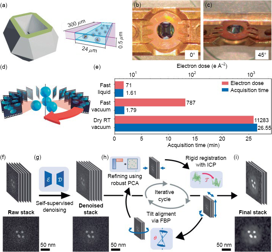
Figure 25. The study in this example utilizes the K-kit liquid pool chip to establish a rapid electron tomography technique, and conducts quantitative three-dimensional structural analysis of small colloidal assemblies in the original liquid environment. (a) Schematic diagram of the K-kit liquid pool chip used for experimental research; (b-c) Appearance of the K-kit chip loaded on a uniaxial tomography support, with tilt angles of 0° and 45° respectively; (d) Method for collecting the tilt sequence of liquid-phase rapid electron tomography: continuously tilting the sample while recording the projection images of the sample; (e) Comparison of the time and electron dose required for rapid electron tomography in liquid and vacuum, as well as conventional room-temperature dry electron tomography in vacuum; (f-i) Preprocessing workflow for the rapid electron tomography tilt sequence; (g) Schematic diagram of denoising using a convolutional autoencoder (CAE) with self-supervised learning; (h) Overview of the adopted reconstruction process; (i) Final processed stacked image, refined, aligned, and denoised.(11))
In addition, recent important application studies also include: using K-kit to induce crystal growth under TEM electron beam and reconstruct its three-dimensional image.(12)Explore the distribution and characteristics of active nanoparticles in beauty products.(13)and the research observation and preparation method development of anticancer drug nanocrystals(14)Wait. These research topics are broad and diverse, fully demonstrating the high potential of the K-kit in the field of biomedical applications.
4. Application Limitations and Technical Comparison of K-kit and In-situ Liquid TEM Sample Rod
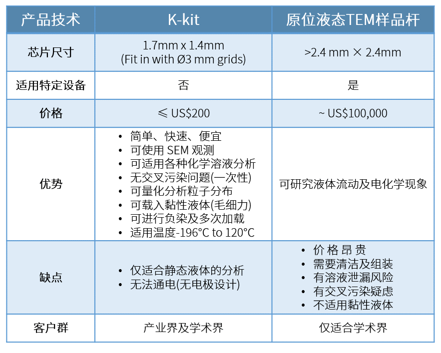
In fact, the K-kit still has certain application limitations in electron microscopy observation of liquid samples. Compared to the in-situ liquid TEM sample holder scheme, the internal storage channel of the K-kit is a closed cavity, making it suitable only for static solution observation and difficult to achieve dynamic research analysis of flowing liquids. Additionally, since the K-kit does not yet have built-in circuits, electrodes, or sensing components, it is also challenging to conduct related research such as micro-area heating observation or electrochemical reactions.
In contrast, the in-situ liquid TEM sample rod has more powerful functions, capable of introducing flowing liquids for dynamic observation in a liquid-phase environment, such as nanoparticle growth, electrochemical reactions, and biomolecular movement. Additionally, its modular liquid cell chip is often equipped with electrode designs, allowing for the application of electric fields in a liquid environment to study the charging and discharging processes of battery electrode materials, electrochemical reaction mechanisms, etc. It can also conduct localized heating through the electrodes to investigate the effects of temperature changes on material dissolution, crystallization, and phase changes. Therefore, the in-situ liquid TEM sample rod is particularly suitable for more in-depth academic research.
However, in industrial applications where rapid acquisition of analytical results is required, or in research scenarios that involve processing a large number of test samples, relying solely on in-situ liquid TEM sample holders may not fully meet the needs. Therefore, it is recommended that users select the most suitable technology based on their analytical objectives, or combine the advantages of K-kit with the in-situ liquid TEM sample holder to establish a liquid nanomaterial detection solution that is both efficient and comprehensive. Table 4 compares the technical characteristics of K-kit and in-situ liquid TEM sample holders for user reference.
Table 4. Comparison of technical characteristics between K-kit and in-situ liquid TEM sample holder
5. Conclusion
The application of K-kit enables high-quality electron microscopy imaging of liquid samples, allowing for direct observation and analysis of nanostructures and their aggregation phenomena, whether for liquid samples in their final product form or general dried samples. K-kit features advantages such as ease of use, rapid detection, and high applicability, and can prepare various types of liquid samples to meet analytical needs. It also achieves unique functions including wet negative staining, multiple loading, lattice diffraction, and composition analysis, making it the only choice on the market suitable for simultaneous application in academic research with complex testing conditions and industrial-related nanofluid analysis.
References
[1] Pu, S., Gong, C., & Robertson, A. W., Royal Society Open Science, 7 (1), 191204 (2020).
[2] Heide, H. G., Journal of Cell Biology, 13, 147 (1962).
[3] Lai, S. E., Hong, Y. J., Chen, Y. T., et al., "Direct-Writing of Cu Nano-Patterns with an Electron Beam", Microsc. Microanal, 21, 1639, (2015).
[4 ]Hong, Y. J., Tai, L. A., Chen, H. J., et al., “Stable Water Layers on Solid Surfaces”, Physical Chemistry Chemical Physics, 18, 5905 (2016).
[5] Trang, N., Chang, J., Chen, W. A., et al, Applied Sciences, 10 (14), 4946 (2020).
[6] Lu, P. J., Fang, S. W., Cheng, W. L., et al., Journal of Food and Drug Analysis, 26, 1192 (2018).
[7] Liu, K.L., Wu, C.C., Huang, Y.J., et al., Lab on a Chip, 8, 1915 (2008).
[8] Tai, L.A., Kang, Y. T., Chen, Y. C., et al, Analytical Chemistry, 84, 6312 (2012).
[9] Kuo, J. C., Tan, S. H., Hsiao, Y. C., et al., ACS Sustainable Chemistry & Engineering, 10, 1, 464 (2022).
[10] Kaczmarczyk, O., Augustyniak, D. & Zak, A., ACS Nano, 19, 12710 (2025).
[11] Arenas Esteban, D., Wang, D., Kadu, A., et al., Nature Communications, 15 (1), (2024).
[12] Das P. P., Cookman, J., Pérez, A. G., et al., Microscopy and Microanalysis, 28, S1, 854 (2022).
[13] Ilett, M., Naveed, E., Roncal-Herrero, T. et al., Journal of Nanoparticle Research, 25, 122 (2023).
[14] Sharma, S. K., Palanikumar, K. L., Pasricha, R., et al., Pharmaceutics, 16 (11), 1471 (2024).
[15] Kawamoto, H., Wakui, A. & Tamura, K., et al., "Image sharpening by the ES-Corrector for TEM observation of specimen in-liquid," In proceedings of 13th Asia Pacific Microscopy Congress, Brisbane, Australia, February 2-7, (2025).
[16] "MA-tek K-kit Services." MA-tek Inc., please refer to the website: www.matek.com/services/index/K-kit. Accessed May 8, (2025).
[17] “Hummingbird Scientific Homepage.” Hummingbird Scientific Inc., please refer to the website: www.hummingbirdscientific.com/. Accessed May 8, (2025).
[18] “Protochips Solutions.” Protochips Inc., please refer to the website: www.protochips.com/solutions/. Accessed May 8, (2025).
Author Biography
Mr. Chen Hong-ren is a PhD from the Institute of Aerospace Engineering at National Cheng Kung University and is currently the Director of the R&D Center at MA-tek.
Hung-Jen Chen received his Ph.D. in the Institute of Aeronautics and Astronautics from National Cheng Kung University. He is currently serving as the Director of the R&D Center at MA-tek Inc.


