
3D IC packaging: Development of heterogeneous bonding technology and process design assisted by in-situ heated atomic force microscopy.
3D IC Packaging: Development of Heterogeneous Bonding Technology and Process Design Assisted by In-Situ Heating Atomic Force Microscopy
Professor Chen Zhi, PhD student Lin Huai'en
National Yang Ming Chiao Tung University, Department of Materials Science and Engineering
-
3D IC packaging and heterogeneous bonding technology
In recent years, the rapid growth of the artificial intelligence and high performance computing markets has driven semiconductor technology towards higher performance and lower power consumption. Generally, the enhancement of chip performance can be achieved by reducing transistor sizes; however, as the sizes continue to shrink, quantum tunneling phenomena lead to leakage currents, exacerbating power consumption. To overcome this predicament, 3D ICs, which are fabricated with a vertical transistor architecture, such as FinFETs and GAAFETs, have become a prominent trend in CMOS technology development and have been successfully applied in the market. However, as CMOS technology nodes shrink, the length and complexity of interconnect wires in the back-end of line (BEOL) processes increase significantly, resulting in a substantial rise in wire delay, which becomes a bottleneck for further enhancement of chip performance.Figure 1In addition, the complexity of 3D IC architecture keeps the costs of processes and research and development high. To address these issues, 2.5D/3D IC packaging technology has emerged, which integrates chips with different functions to a higher degree, shortening signal transmission paths and thereby reducing overall power consumption. Among them, 3D IC packaging technology has advantages in system integration, volume, and performance, and can effectively reduce unit costs, making it a key technology for continuing Moore's Law (More than Moore).Figure 2)。
-
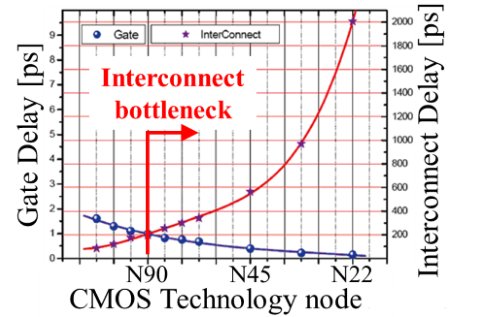
Figure 1. The relationship between gate and wire delay as CMOS technology nodes evolve, where wire delay has become a bottleneck for chip performance improvement [2].
-
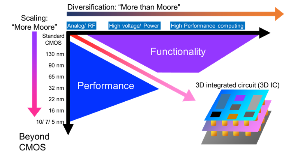
Figure 2. Three-dimensional integrated circuits are packaged in a vertical direction, achieving a high degree of integration of chips with different functions, resulting in system-level performance improvements, thereby continuing Moore's Law.
In 3D IC packaging technology, the vertical stacking of chips is a key process. Currently, the mainstream method for chip stacking still relies on solder bumps. However, with the shrinking of interconnect pitch, solder bump technology faces numerous reliability issues, such as necking, depletion, and collapsing. Therefore, to overcome these challenges, heterogeneous bonding technology has emerged. Compared to solder bumps, heterogeneous bonding technology can simultaneously form an insulating dielectric layer and a metal wire layer in a single process, achieving high-density and low-resistance interconnections, and further reducing power consumption. As a result, this technology has been widely adopted by several semiconductor companies, such as Sony, which incorporated it into CMOS image sensors in 2016.Figure 4), being the first product in the industry to use heterogeneous bonding technology, Advanced Micro Devices (AMD) announced its first server processor applying this technology in 2022, utilizing TSMC's SoIC technology, effectively reducing power consumption(Figure 5With the mass production of heterogeneous bonding, the importance of 3D IC packaging is increasing day by day.
__25K127ym9f.png "03 (2)")
Figure 3. Reliability issues caused by the miniaturization of solder bump size and spacing [4, 5].
-
__25K12aoXl6.png)
Figure 4.Sony uses heterogeneous bonding technology to produce CMOS image sensors in the Samsung Galaxy S7 camera.
-
__25K12mO0ZA.png)
Figure 5. AMD released its first server processor using heterogeneous bonding technology. [Source: AMD]
Heterogeneous bonding technology can achieve high-density interconnections and improve chip performance; however, its unique bonding mechanism presents many process challenges. The mechanism is shown in Figure 6. First, copper/silicon dioxide embedded via holes (Cu/SiO2Alignment of the upper and lower wafers (or chips) is performed via damascene, followed by the bonding of the dielectric layer at room temperature. Finally, during high-temperature annealing, the mismatch in thermal expansion coefficients between copper and silicon dioxide causes the copper pads to expand and contact the opposing copper pads, completing the copper-to-copper bonding. Due to the nanometer-level expansion of the copper pads during annealing, the challenge of preparing copper/silicon dioxide embedded vias is severe. If over-polishing occurs during the chemical mechanical planarization (CMP) process, the copper pads will be unable to complete the bonding during subsequent annealing, leading to process failure.Figure 6bTherefore, precise CMP control and understanding the thermal expansion of copper pads at high temperatures are crucial for improving the yield of heterogeneous bonding processes. Previous related studies could only simulate the thermal expansion of copper pads at high temperatures using methods such as finite element analysis (FEA), lacking direct measurement methods for verification. To address this deficiency in related technology, our research team proposed using in-situ heating atomic force microscopy (in-situ AFM) to observe the surface morphology of copper pads under heating conditions, successfully obtaining the actual expansion amount, which is a first in related research. With this data, we can grasp the process window of heterogeneous bonding-related processes, such as the Cu recess during CMP control and annealing temperature, and verify the accuracy of simulation values, marking a significant breakthrough for related applications.
__25K12aFFlP.png "06 (2)")
Figure 6. The process flow of heterogeneous bonding, including wafer (or chip) alignment, achieving dielectric bonding at room temperature, and completing copper-to-copper bonding through post-annealing. (a) Optimization of copper pad recess and (b) situation of excessive copper pad recess [10].
The principle of using in-situ heating atomic force microscopy
Atomic Force Microscopy (AFM) is commonly used to analyze surface morphology, with its main components including a cantilever with a probe, a piezoelectric scanner, a laser light source, and a photodetector. The basic principle of AFM is to use the probe to scan the sample surface, with the photodetector receiving the laser signal and detecting changes in the probe's position, thereby mapping the surface morphology. AFM mainly has three types: contact mode, non-contact mode, and tapping mode, each suitable for different application scenarios. Among them, tapping mode is widely used for surface morphology analysis due to its highest spatial resolution.
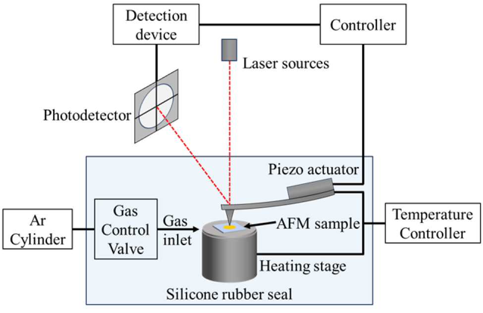
Based on the working principle of tapping mode AFM, as long as the resonance frequency and amplitude of the cantilever are kept stable during measurement, AFM can be performed in a heated environment. This study uses the Dimension ICON from Bruker Inc., which includes a heated sample stage and cantilever, a gas control system, and a rubber cover, such asFigure 7As shown. The measurement range of this study is from room temperature (RT) to 200°C, and each test temperature is maintained for 15 minutes to achieve thermal equilibrium before scanning, avoiding thermal drifting effects. In order to reduce errors caused by the temperature difference between the probe and the sample surface, both the sample and the cantilever need to be heated to the same temperature during measurement. Additionally, to prevent oxidation of the copper pad surface, a stable flow of argon (Ar) gas is continuously injected into the rubber cover during the measurement process.
Using In-situ AFM to Assist in Heterogeneous Bonding Process Design
This research utilizes in-situ AFM to record the surface morphology of copper/silicon dioxide embedded via holes at different temperatures, such asFigure 8As the temperature rises, the color of the copper pads changes from dark brown to light white, indicating that the height of the copper pad surface increases with the temperature. The same result can also be seen in the expansion curve graph of the cross-section.Figure 8bobserved.Figure 8cThe height difference between the copper and silicon dioxide surfaces at different temperatures shows that the copper pad is recessed about 6 nanometers compared to the silicon dioxide surface at room temperature, and protrudes above the silicon dioxide surface at 150°C, reaching a protrusion of about 4 nanometers at 200°C. This result is the first study to verify the mechanism of heterogeneous bonding through direct measurement, indicating that the copper pad expands from a recess to a protrusion. Furthermore, bonding was successfully completed at the conversion temperature (150°C) of the copper pad from recess to protrusion. This study successfully utilized in-situ AFM to assist in the process design of heterogeneous bonding.
-
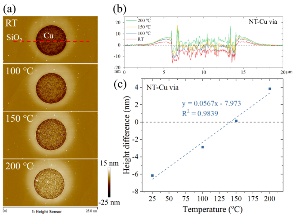
Figure 8. Surface morphology of copper/silicon dioxide embedded via holes measured from room temperature to 200°C: (a) top view and (b) cross-sectional view, (c) height difference of copper and silicon dioxide surfaces at different temperatures.
-
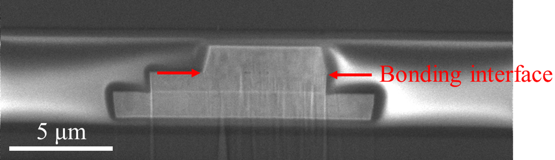
Figure 9. The test sample successfully completed bonding at the conversion temperature of the recessed protrusion (150°C).
Utilizing nanocrystalline copper to enhance its thermal expansion within silicon dioxide pores and applying it to heterogeneous bonding.
In heterogeneous bonding, the process accuracy of chemical mechanical planarization (CMP) directly affects production yield. However, with the miniaturization of dimensions and interconnection spacing, the thermal expansion of copper pads becomes increasingly smaller, making the requirements for CMP accuracy increasingly impractical. Therefore, enhancing the expansion amount has become another approach. Relevant literature has suggested that alloying copper pads or adding an additional capping layer can increase the expansion amount by about 40%. However, this approach may lead to the formation of intermetallic compounds (IMC) or increased resistance, and does not comply with existing processes. To address this dilemma, our team utilized the concept of grain-boundary engineering to produce nanocrystalline copper (NC-Cu) through electroplating, successfully increasing the expansion amount by over 100%.
Figure 10For the backscattered electron diffraction observation of general copper and nanocrystalline copper, by adding a grain-refining additive during electroplating, the grain size of the copper pads is reduced to about 100 nanometers, as measured by the temperature-dependent surface morphology results from in-situ AFM.Figure 11The degree of expansion of nano-crystalline copper can be observed to be quite significant, as seen from the expansion curve of the cross-section.Figure 12It can also be observed that the expansion of nano-crystalline copper can exceed 100% compared to regular copper. From the statistically significant cumulative distribution graph(Figure 13The expansion amount of nano-crystalline copper is significantly greater than that of general copper, indicating its high potential to enhance the process window of heterogeneous bonding. In addition, from the cumulative distribution map ( Figure 13It can also be understood that the expansion of copper pads follows a normal distribution, and the lower limit of the expansion amount is the process window of heterogeneous bonding, which is an important value that simulations cannot provide.
-
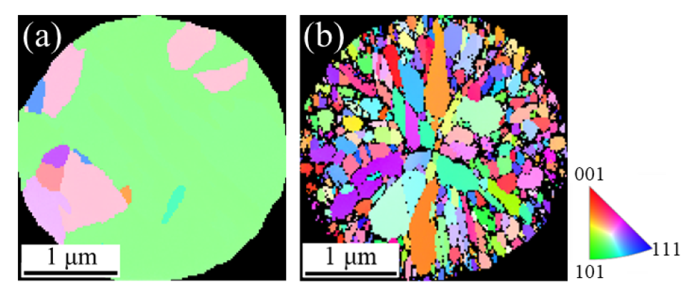
Figure 10. (a) Backscattered electron diffraction top view of ordinary copper and (b) nanocrystalline copper [14].
-
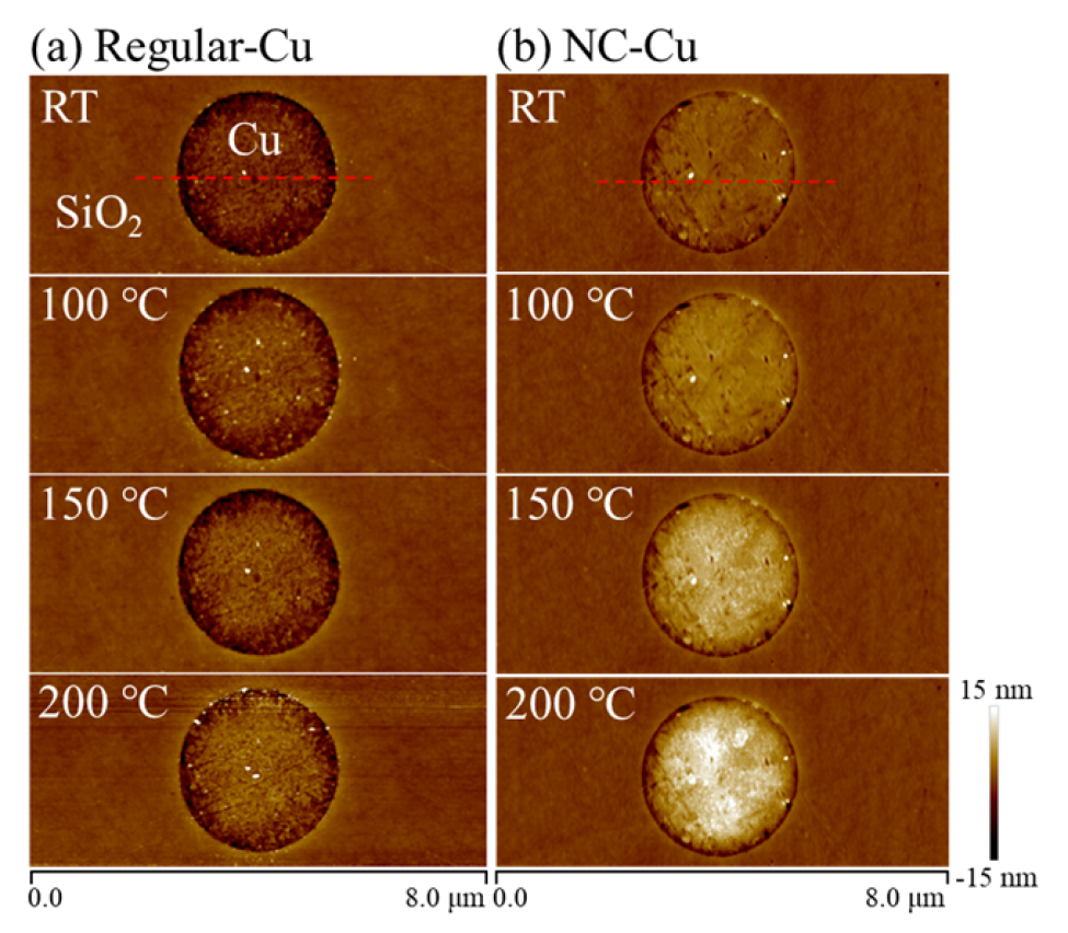
Figure 11. (a) Surface morphology of conventional copper and (b) nanocrystalline copper measured from room temperature to 200°C [14].
-
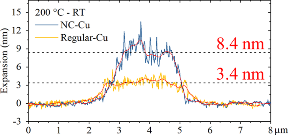 Figure 12. Cross-sectional expansion curves of conventional copper and nanocrystalline copper at 200°C [14].
 -
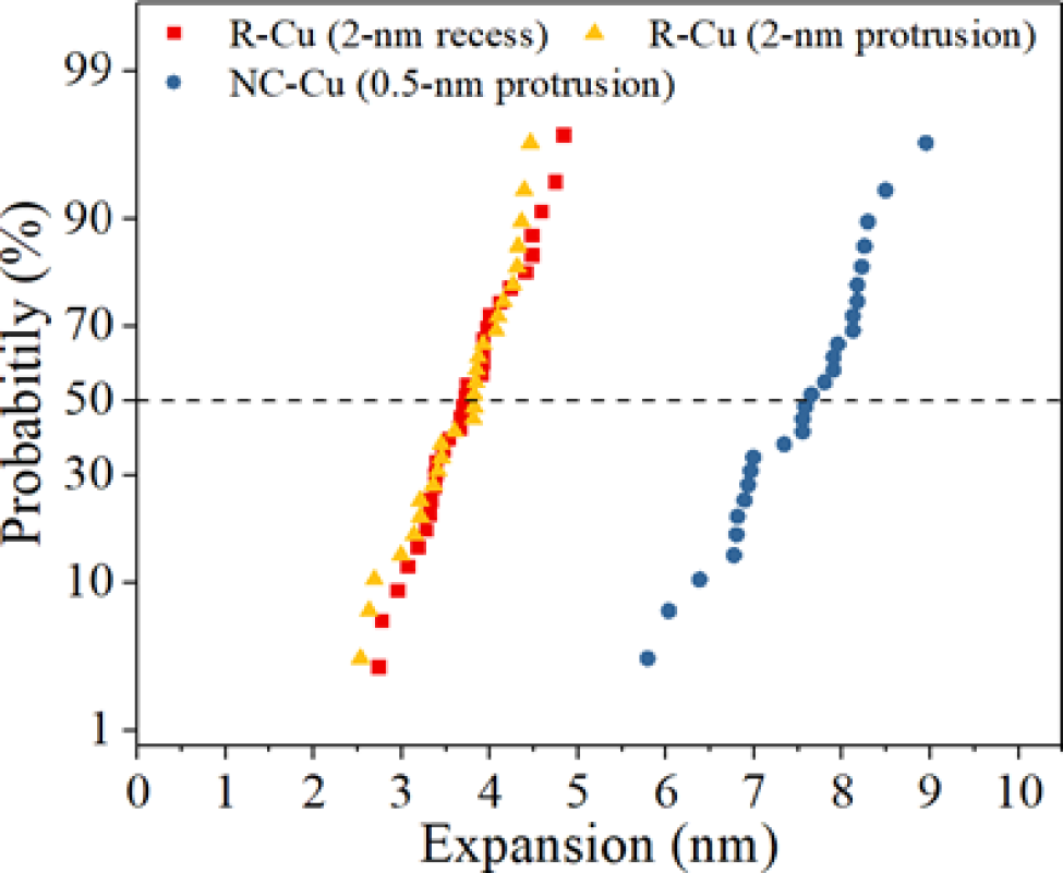 Figure 13. Cumulative distribution of expansion amounts of regular copper and nanocrystalline copper [14].
Technical Outlook
With the expansion of the semiconductor market, 3D IC packaging has become key to enhancing chip performance. However, the core process - heterogeneous bonding - still faces many technical challenges, such as the reduction in thermal expansion of copper pads caused by size scaling, which in turn affects bonding reliability and yield. To address these issues, the research team utilized in-situ heating atomic force microscopy (AFM) to directly measure the surface morphology of copper/silicon dioxide embedded vias at different temperatures, obtaining statistically significant data on copper pad expansion and determining the process window for heterogeneous bonding. Furthermore, through grain boundary engineering, we successfully reduced the grain size of copper pads to the nanoscale, significantly enhancing their thermal expansion behavior, resulting in an expansion increase of over 100%, and meeting current semiconductor processes. This breakthrough in technology demonstrates its high application potential in fine-pitch heterogeneous bonding.
Reference:
[1] R.W. Keyes, Physical limits of silicon transistors and circuits,Reports on Progress in Physics, 68 (2005) 2701.
[2] M.R. Baklanov, C. Adelmann, L. Zhao, S. De Gendt, Advanced interconnects: materials, processing, and reliability, ECS Journal of Solid State Science and Technology, 4 (2015) Y1-Y4.
[3] W. Arden, M. Brillouët, P. Cogez, M. Graef, B. Huizing, R. Mahnkopf, More-than-Moore white paper, Version, 2 (2010) 14.
[4] C. Chen, D. Yu, K.-N. Chen, Vertical interconnects of microbumps in 3D integration, MRS bulletin, 40 (2015) 257-263.
[5] K. Oi, S. Otake, N. Shimizu, S. Watanabe, Y. Kunimoto, T. Kurihara, T. Koyama, M. Tanaka, L. Aryasomayajula, Z. Kutlu, Development of new 2.5 D package with novel integrated organic interposer substrate with ultra-fine wiring and high density bumps, 2014 IEEE 64th Electronic components and technology conference (ECTC), IEEE, 2014, pp. 348-353.
[6] Y. Kagawa, N. Fujii, K. Aoyagi, Y. Kobayashi, S. Nishi, N. Todaka, S. Takeshita, J. Taura, H. Takahashi, Y. Nishimura, Novel stacked CMOS image sensor with advanced Cu2Cu hybrid bonding, 2016 IEEE International Electron Devices Meeting (IEDM), IEEE, 2016, pp. 8.4. 1-8.4. 4.
[7] E. Beyne, S.-W. Kim, L. Peng, N. Heylen, J. De Messemaeker, O.O. Okudur, A. Phommahaxay, T.-G. Kim, M. Stucchi, D. Velenis, Scalable, sub 2μm pitch, Cu/SiCN to Cu/SiCN hybrid wafer-to-wafer bonding technology, 2017 IEEE International Electron Devices Meeting (IEDM), IEEE, 2017, pp. 32.34. 31-32.34. 34.
[8] S. Furuse, N. Fujii, K. Kotoo, N. Ogawa, S. Saito, T. Yamada, T. Hirano, Y. Hagimoto, H. Iwamoto, Behavior of Bonding Strength on Wafer-to-Wafer Cu-Cu Hybrid Bonding, 2022 IEEE 72nd Electronic Components and Technology Conference (ECTC), IEEE, 2022, pp. 591-594.
[9] M.-K. Kim, S. Park, A. Jang, H. Lee, S. Baek, C. Lee, I. Kim, J. Park, Y. Jee, U.-B. Kang, Characterization of die-to-wafer hybrid bonding using heterogeneous dielectrics, 2022 IEEE 72nd Electronic Components and Technology Conference (ECTC), IEEE, 2022, pp. 335-339.
[10] H.-E. Lin, W.-L. Chiu, H.-H. Chang, Y.-T. Yang, C. Chen, Revealing challenges of downscaling effects on Cu thermal expansion in advanced hybrid bonding using in-situ AFM, Applied Surface Science, (2025) 162539.
[11] B. Bhushan, Nanotribology and nanomechanics: an introduction, Springer, 2008.
[12] H.-E. Lin, D.-P. Tran, W.-L. Chiu, H.-H. Chang, C. Chen, In-situ measurement of thermal expansion in Cu/SiO2 hybrid structures using atomic force microscopy at elevated temperatures, Applied Surface Science, 662 (2024) 160103.
[13] S. Dag, M. Liu, L. Jiang, A. Kiaee, G. See, P. Lianto, B. Ayyagari-Sangamalli, E.M. Bazizi, Development of copper thermal coefficient for low temperature hybrid bonding, 2023 IEEE 73rd Electronic Components and Technology Conference (ECTC), IEEE, 2023, pp. 342-349.
[14] H.-E. Lin, D.-P. Tran, W.-L. Chiu, H.-H. Chang, C. Chen, Enhanced thermal expansion with nanocrystalline Cu in SiO2 vias for hybrid bonding, Applied Surface Science, 672 (2024) 160784.


