
Let's explore the world of planes---Introduction to two-dimensional materials
Let's explore the world of planes---An introduction to two-dimensional materials.
Professor Li Wenxi
Doctoral student Chen Shih-Hsun
Department of Electrical Engineering, National Cheng Kung University
(This article is written by Professor Li Wenxi and PhD student Chen Shixun; edited by MA-tek)
-
Current Applications of Two-Dimensional Materials
The 2010 Nobel Prize in Physics was awarded to the discoverers of graphene, Andre Geim and Konstantin Novoselov from the University of Manchester in the UK. In 2004, they successfully peeled graphene from a block of graphite using 3M tape, sparking a research boom in the field of two-dimensional materials. Utilizing the various interesting properties of two-dimensional materials, graphene has brought disruptive products to our lives, ranging from seawater desalination, electric vehicle supercapacitors, to textiles.
Graphene's surface repels water, and utilizing this property allows water to quickly penetrate its capillary channels. By further using epoxy encapsulant to limit the expansion of graphene's capillary channels (GO) after soaking in water, a screening effect can be achieved, preventing salt from passing through and filtering out up to 97% of the salt in water. (Figure 1)
When applied to battery electrodes, graphene can effectively enhance the charging and discharging efficiency and energy density of batteries. Traditional electrode materials require additives such as glue, which reduce conductivity, resulting in unsatisfactory charging and discharging rates. Additionally, the functional groups on the electrode materials can react with the electrolyte at higher voltages, limiting the energy density that can be input. Graphene can address both of these issues; its surface lacks functional groups and can be directly grown on substrates without adhesives, compensating for the two major drawbacks of supercapacitors and significantly shortening charging times for electric vehicle batteries. (Figure 2)
Activated carbon has been widely used in textiles for antibacterial and deodorizing purposes. At the two-dimensional scale, carbon—graphene, with its strength, ductility, and high electrical and thermal conductivity, adds new features to textiles. It can be mixed into the fabric fibers to diffuse absorbed heat throughout the garment for uniform temperature, or it can be coated to create small exothermic circuits to drive away cold.
In addition to graphene composed of carbon elements in two-dimensional material systems, there are many materials composed of other elements waiting to be explored, which will add various magical functions to everyday products.
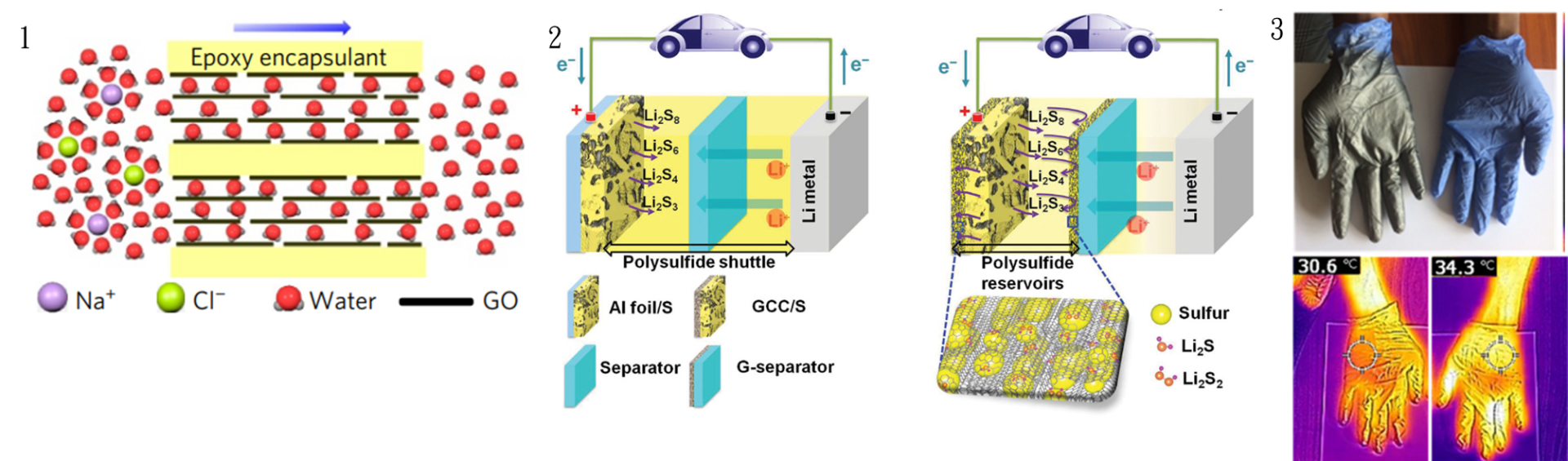
Figures 1-3. Current applications of two-dimensional materials [1] [2] [3]
two-dimensional materials
The arrangement of materials' lattice structures is divided into zero to three-dimensional materials according to points, lines, surfaces, and bodies. The three-dimensional blocks commonly seen in life are composed of three dimensions: length, width, and height. Two-dimensional materials are planar layered materials composed of two dimensions: length and width.
When we control a material to such a two-dimensional sheet size through process technology, the material's characteristics are significantly different compared to the common three-dimensional stacking method.
__26D20zG5SI.png "4 (1)")
Figure 4. Material lattice dimensions
First, most of the atoms in the material are exposed to the external environment, giving it a large effective surface area for chemical reactions, which is advantageous in the field of catalysis. Second, the bonding positions in two-dimensional layered materials lack vertical dangling bonds, reducing interference at the interface with other materials, and thus requiring less passivation processing. Furthermore, the impact of thickness means that the material has only one layer of molecules in the vertical direction, eliminating the interactions and bonds of a large number of molecular atoms that occur during three-dimensional stacking, allowing the weak van der Waals forces to dominate in two-dimensional materials. When different two-dimensional materials are stacked together, the layers are also connected by this force, referred to as van der Waals heterostructures. (Figure 5) The second impact of low layer thickness is the change in the band gap; for example, molybdenum disulfide has an indirect band gap of 1.2 eV in multilayer form, while it transforms into a direct band gap of 1.8 eV in monolayer form, thus exhibiting different optical, electrical, and semiconductor properties.
The family of two-dimensional materials exhibits a wide range of properties, including metals, semi-metals, semiconductors with various energy bands, and insulators. Similar to three-dimensional materials, various types of two-dimensional materials can be combined to create a variety of components. (Figure 5) [10]
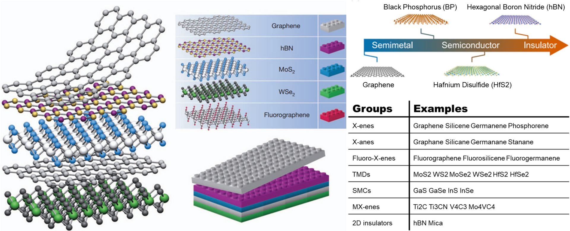
Figure 5. (a) Van der Waals heterostructure stacking [5] (b) Common two-dimensional materials [10]
Two-dimensional materials applied in electronic component transistors
The demand for technological development today is trending towards high-speed computing with large amounts of data. Over the past forty years, photolithography technology has continuously defined smaller patterns, achieving increased operating speeds and reduced power consumption with smaller transistor sizes. When the channel length is reduced to below ten nanometers, derivative problems arise, leading to a sharp decline in transistor performance, including severe leakage current, decreased threshold voltage, increased subthreshold swing, carrier surface scattering, velocity saturation, and hot carrier effects, collectively known as short channel effects.
The semiconductor development blueprint IRDS plans to continue shrinking the dimensions of computing components. FinFETs and gate-all-around structures have been proposed to enhance gate control and limit leakage current. Nowadays, silicon bulk materials have shrunk to physical limits, resulting in a significant reduction in carrier mobility and still relatively high leakage current. The source-drain ohmic contact is also not ideal due to complex processes, making it urgent to explore new systems and materials.
The most widely studied emerging two-dimensional semiconductor materials are transition metal dichalcogenides (TMDs), primarily composed of molybdenum and tungsten, combined with chalcogen elements such as sulfur, selenium, and tellurium. At advanced process scales below two nanometers, TMDs can provide higher carrier mobility and extremely low leakage current compared to silicon-based three-dimensional bulk materials, making them suitable for low-power targets.
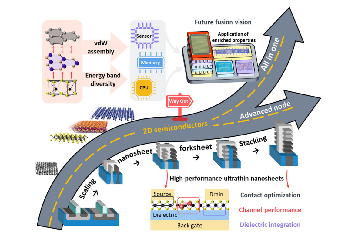
Figure 6. The potential applications of two-dimensional materials in electronic components [14]
Various two-dimensional semiconductor structured transistors have been manufactured and discussed (Figures 6 and 7). Regardless of how the structure is adjusted or changed, the basic structure remains the same. Current flows through the channel, from the channel into the source-drain metal wires, and the gate controls whether the current passes through or not. The following topics need to be discussed in order: (1) Channel modulation (2) Ohmic contact (3) Dielectric material integration.
The core indicator of the transistor channel is current efficiency, which depends on the channel material having suitable effective mass and energy bands. After selecting the channel material, modulation is carried out to achieve precise control over its electrical, optical, and magnetic performance through doping engineering. The process techniques will be discussed in the material post-processing section.
The effective mass of the material is inversely proportional to the maximum current that can be passed through. Materials with lower effective mass can provide higher current limits. However, the effective mass cannot be too low, as it can easily lead to induced tunneling current between the source and drain, causing current to appear in the off state where there should be no current signal, resulting in incorrect calculations by this operational component. The MoS2 from the family of two-dimensional semiconductor TMDs has a relatively large effective electron mass of about 0.5 m0, which can effectively suppress the direct tunneling of current between the source and drain in ultra-thin channel devices, effectively mitigating the leakage current issue.
The band gap directly affects the ratio between the on-state current and the off-state leakage current. TMDs have a direct band gap in monolayer form, and as the number of layers increases, the band gap of TMDs gradually decreases and changes from a direct band gap to an indirect band gap, ranging from 1.1 to 2.1 eV. In addition to TMDs, black phosphorene (BP) is also a potential channel material that has attracted attention, with a tunable band gap from 0.3 eV to 2.0 eV, all of which are direct band gaps. Another difference from traditional silicon semiconductors is that two-dimensional materials naturally exhibit n-type, p-type, or bipolar characteristics without doping. For example, the most widely studied MoS2 is n-type, black phosphorus and MoTe2 are p-type, and WSe2 can operate in a bipolar manner.

Figure 7. Potential structure of two-dimensional material devices, the left image is a Complementary FET (CFET) [15], and the right image is a Tunnel Field Effect Transistor (TFET) [16].
__26D20grUBy.png "8 (1)")
Figure 8. Engineering of Ohmic contacts for two-dimensional materials, the left image uses a semimetal as the contact point [17], the middle and right images illustrate the Fermi level pinning situation [18].
Ohmic contact engineering in semiconductors primarily addresses the issue of electronic transport at the interface of adjacent dissimilar materials. When electrons traverse the metal-semiconductor interface, a significant impedance arises that makes it difficult for current to flow, and this type of material contact is referred to as Schottky contact. The phenomenon occurs due to the mismatch of work function and Fermi level between metal and semiconductor materials, where free electrons and holes continuously transfer in this region until the Fermi level reaches equilibrium. This process obstructs the external input current, known as the phenomenon of Fermi level pinning. Two strategies have been proposed to resolve this issue: heavily doping the semiconductor or introducing a thin dielectric layer at the interface to decouple the metal-semiconductor interaction. The first strategy is quite challenging for two-dimensional materials in terms of processing technology, while the second structure is dominated by a lower impedance tunneling barrier, which still does not meet the demand for small linewidth devices.
The third strategy has recently been proposed, using semi-metal - semiconductor contacts to suppress metal-induced gap states (MIGS) to avoid gap state pinning. [17] (Figure 8 left) By aligning the Fermi level of the semi-metal with the minimum of the conduction band of the semiconductor, the MIGS contribution from the conduction band is greatly reduced. This makes the MIGS completely contributed by the valence band, allowing it to be filled and saturated, achieving gap-state saturation and realizing Ohmic contact. MoS2 devices paired with the complementary semi-metal Bi achieved excellent performance, with a contact resistance of 123 ohm-microns and a drain current density of 1,135 microamperes/micron.
The dielectric material placed between the gate and the channel also has a critical impact on the electrical performance of the transistor. Improving the quality of the dielectric layer can reduce the threshold voltage (Vth), which is beneficial for lowering the power consumption of the device; it can also reduce hysteresis, which is advantageous for the stability of the device. In silicon processes, the process technology of high-k dielectric material hafnium oxide has matured. However, when applied to two-dimensional material transistors, new process challenges arise. The surface of two-dimensional materials is clean without dangling bonds, eliminating the issue of passivating dangling bonds. The new issue is that there are no nucleation points for the deposition of dielectric materials, resulting in uneven film formation. Charges flowing through the channel being trapped by defects in the dielectric layer can lead to hysteresis and leakage problems in the device.
To adhere to smooth inert surfaces, selecting two-dimensional materials with van der Waals surfaces as an insulating layer is a possible solution. The use of hexagonal boron nitride (h-BN) not only serves as a gate dielectric layer but can also act as a packaging material, isolating two-dimensional semiconductors from the external environment, significantly improving intrinsic properties such as mobility and stability. Currently, the growth of h-BN remains a challenge, and research has used transfer methods to manufacture single devices to verify principles, but large-scale production is still not feasible. In addition, the dielectric constant of h-BN is about 5, similar to that of silicon dioxide, which is a non-high-k dielectric. There will be leakage current when gate control capability requires a smaller effective oxide thickness (EOT). Another proposed solution is to deposit a seed layer on the channel to connect with the dielectric layer, and the effects of Y2O3 and organic PTCDA have been discussed.
The material performance of two-dimensional materials can adapt to existing structures and meet future demands. To achieve large-scale integrated applications, more research on processing techniques is needed to enhance the uniformity of performance over large areas.
Two-dimensional materials applied in optoelectronic devices
Optoelectronic devices can be divided into photodetectors that absorb light as a switch signal, solar cells (or photovoltaic devices) that convert absorbed light into electrical energy, and light-emitting devices (the most common being light-emitting diodes, LEDs) (Figure 10)[27]. The main indicators of device performance include high responsivity, short response time, high sensitivity, large photo gain, and linearity of responsivity changes.
In light-absorbing devices, three steps can be discussed: (1) light absorption, (2) generation of charge carriers, and (3) charge carrier transport. The goal of material light absorption is to cover a large receiving bandwidth, depending on the material's energy band. Two-dimensional semiconductor materials can receive light signals that cover a wide bandwidth range, with corresponding materials available from mid-infrared to visible light. However, two-dimensional atomic layer materials have relatively less light absorption compared to three-dimensional bulk materials. The efficiency of receiving different frequency bands can be increased by stacking two-dimensional material heterostructures, and the design of the devices needs to focus on enhancing gain.
In the stage of photogenerated carriers, the material absorbs light to produce carrier-electron hole pairs. To increase the gain, it is important to reduce the recombination of electron-hole pairs, which can increase the number of extracted carriers. A common approach is to add another material to guide the carriers to move in different directions. For example, in reference [7], indium atoms are adsorbed and placed above the two-dimensional semiconductor tungsten disulfide (WS2) to guide the photogenerated electrons to transfer to the tungsten disulfide channel, while the holes are trapped by the indium atoms.
The main challenge of carrier transport lies in the interface between the semiconductor channel and the metal wire, where contact resistance causes consumption and leads to low responsivity. Since no method has yet emerged to repair the damage that occurs in two-dimensional materials during traditional doping processes, choosing a metal that matches the band structure and utilizing quantum tunneling mechanisms are currently the main approaches to reducing contact resistance. Graphene, which has semi-metallic properties, is often used to bridge two-dimensional material semiconductors and metal wires, as it can form low contact resistance with two-dimensional materials. Moreover, its ultra-high carrier mobility characteristics further reduce the likelihood of separated electron-hole pairs recombining.
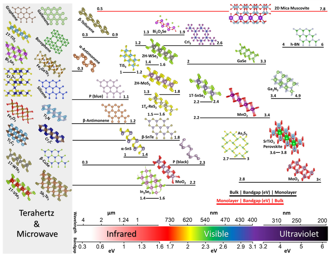
Figure 9. Two-dimensional materials applicable in various frequency bands [6]
__26D20aaweD.png "10 (1)")
Figure 10. Common structures of optoelectronic devices [27]
Currently popular light-emitting devices mainly apply the principles of photoluminescence (PL) and electroluminescence (EL). Structures using direct current power include light-emitting diodes (LEDs) and quantum dots (Quantum dot LED, QLED) for single photon emission. The characteristics of two-dimensional materials have many advantages in light-emitting devices. The complex process of QLED and its dependence on hydrophobic insulating long ligands hinder their stability and conductivity, while the self-terminated surface characteristics of two-dimensional materials allow their devices to operate without interference from ligands. The low carrier transport capability and exciton recombination ability of organic light-emitting diodes (OLEDs) hinder brightness improvement, while the excellent exciton luminescence capability of two-dimensional semiconductor TMDs can achieve high brightness at room temperature.
The quantum confinement effect occurring in thin layer materials will reduce the density of states and carrier concentration of thin layer three-dimensional materials. Two-dimensional semiconductor TMDs, due to their high effective mass, bring about high carrier concentration, under such conditions, higher-order excitonic quasi-particles can be observed, such as excitons and charged excitons (trions), etc. Two-dimensional semiconductor TMDs have strong Coulomb interactions, which tightly bind their excitons, resulting in high exciton binding energy, which can even be observed at room temperature. The binding energy of typical III-V semiconductor GaAs is 4.76 meV, and excitons can only be observed at low temperatures, while the binding energy of molybdenum disulfide MoS2 in two-dimensional TMDs is 240 meV.
Defects in traditional semiconductors can capture carriers, hindering the recombination of electrons and holes, significantly reducing the photoluminescence quantum yield (PLQY), which is a key indicator of the optoelectronic performance of devices. Two-dimensional semiconductor TMDs typically have a higher density of native defects after processing, and repairing these defects is a major technological challenge. However, research has found that neutral exciton recombination is radiative, and high PLQY performance can still be achieved even in the presence of a high defect density, giving two-dimensional TMDs great potential in optoelectronic applications.
In addition to the aforementioned DC input LED structure, a structure using AC power supply has also been proposed (Figure 11)[9]. Through the appropriate switching frequency of the AC power with suitable materials, positive and negative charges meet and combine in the material to emit light. The LED structure emits light through the PN interface of the material, and the narrow material interface and complex structure limit large-area applications. The structure in Figure 11 is simple and is less affected by the Schottky barrier at the material interface, providing a solution for large-area transparent displays.
In the issue of heterogeneous integration between components of different materials and control circuits, two-dimensional materials also have advantages. The control circuits primarily use silicon-based CMOS circuits. Components made of HgCdTe and group III-V elements face challenges during integration with control circuits due to lattice mismatch, which leads to poor bonding. However, two-dimensional materials can be transferred to other materials through a transfer process and adhere to other materials via van der Waals forces, without relying on lattice matching. This characteristic can also be used to create control circuits based on two-dimensional materials for group III-V displays and for transparent and flexible wearable displays. Furthermore, regarding the limited light absorption of two-dimensional materials, research has fortunately found that extending the interaction length can significantly enhance the interaction between the two-dimensional material layers and the optical mode fields propagating along the optical waveguide. With the enhanced interaction between light and matter, the potential applications of optoelectronic devices that integrate silicon and two-dimensional materials through waveguides in various functional photonic integrated circuits have attracted widespread attention.
__26D20agzwP.png "11 (2)")
Figure 11. On the left is an AC LED, and on the right is a photonic device integrating silicon and two-dimensional materials.
Preparation of two-dimensional materials
Common methods for producing materials that are only a few layers thick can be divided into the following types: exfoliation, chemical vapor deposition (CVD), and post-annealing.
The exfoliation method introduces an appropriate amount of force to overcome the weak van der Waals forces between the layers of two-dimensional layered materials, separating large bulk materials stacked in multiple layers into several few-layer sheets, while the covalent bonds, ionic bonds, or metallic bonds within the layers are strong enough to keep the two-dimensional layers intact. For example, ultrasonic treatment and high-shear mixing are direct methods for producing two-dimensional materials in the liquid phase by introducing shear forces. The electrochemical exfoliation method achieves its effect by introducing an electric field to increase the distance between the layers.
The principle of chemical vapor deposition is to use high temperatures to vaporize solid raw materials, causing the raw vapor to undergo gas-phase chemical reactions and deposit onto the target substrate. Taking the two-dimensional semiconductor molybdenum disulfide as an example, solid powders of molybdenum trioxide and sulfur are heated to 600~800°C, and after the gas-phase reaction, a molybdenum disulfide thin layer is formed on the substrate. The challenge lies in suppressing vertical deposition while enhancing horizontal growth. Parameters such as temperature, pressure, holding time, substrate, and precursors have a significant impact on the reaction.
Post-annealing is a two-step growth method, where a precursor is first deposited, and then through post-annealing, it reacts to become the target material, while also enhancing the material's crystallinity to optimize its electrical properties. Sputtering is a method suitable for large-scale manufacturing, belonging to physical vapor deposition (PVD), with advantages of being fast, inexpensive, and scalable, capable of producing tungsten-based two-dimensional materials that usually require higher processing temperatures. However, under the low atomic layer count required for two-dimensional materials, it is difficult to control the precise film thickness, roughness, and crystallinity. Therefore, it is combined with CVD for post-annealing treatment to enhance crystallinity and repair defects.
Post-processing of two-dimensional materials
For the types of performance enhancement control, it is important to choose the appropriate post-processing method for the materials. Common techniques include annealing and doping.
The traditional annealing method is conducted in a vacuum or inert gas environment. Annealing of two-dimensional materials in this environment will result in many defects, such as molybdenum telluride, where the temperature capable of enhancing crystallinity is above 650 degrees, while the tellurium element in the film begins to detach at 250 degrees. Therefore, the annealing of this material must be conducted in an atmosphere filled with tellurium elements, and this characteristic can also be utilized to introduce doped elements into the material during the annealing process (Figure 12-1) [21]. In addition, a method of annealing that is not affected by the atmosphere has been proposed, known as solid phase crystallization (SPC), where a SiO2 cover layer encapsulates the sputtered MoTe2 and is then raised to high temperatures. The solid phase crystallization process can easily be carried out in an atmosphere without Te (Figure 12-2) [22].
__26D204miDo.png "12 (1)")
Figure 12. Post-processing methods for two-dimensional materials (1) Low-temperature annealing (2) Solid-phase crystallization annealing (3) Laser treatment
In the method without additional agents, in addition to the aforementioned annealing, there is also laser treatment. Laser treatment can be applied to specific locations, such as the molybdenum diselenide in Figure 12-3, which transforms from the 2H semiconductor phase to the 1T half-metal phase after laser treatment, and can be applied to the issue of ohmic contact. (Figure 12-3) [23]
In the method of using additives, the main strategies currently used for TMDs doping engineering are (1.) substitutional doping, (2.) charge transfer doping, and (3.) electrostatic field effect doping. Traditional three-dimensional crystalline semiconductors are usually doped with impurity atoms at substitutional or interstitial sites. In contrast, the weak van der Waals interactions between two-dimensional layers lead to larger interlayer distances, which are favorable for the embedding of dopant atoms. Moreover, at such ultra-thin thicknesses, they can also be easily doped through surface charge transfer and external electrostatic field effects.
Substitution doping can be achieved by mixing dopants during the material growth stage, or by introducing dopants into the film after creating vacancies through annealing, plasma, or laser methods. In the presence of sulfur vacancies, doping reactions with group VII (F, Cl, Br) and group V elements (N, P, As) are thermodynamically more likely to occur. At metal sites, the formation of dopants largely depends on the concentration of metal vacancies, such as Re doping in MoS2. Therefore, whether in the growth of defects or in post-processing, using in situ methods makes it relatively easy to implement substitution doping processes.
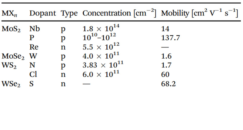
Table 1. Substituted dopants and their effects [25]
__26D20BjtNz.jpg "02 (1)")
Table 2. Dopants and effects of charge transfer doping
Charge transfer doping methods have attracted widespread attention in regulating the electronic behavior of semiconductors. Compared to substitutional doping, which involves the incorporation of foreign dopant atoms into the lattice, charge transfer doping utilizes the charge transfer interactions between the host material and adjacent media (including surface adsorbed atoms, ions, molecules, particles, and substrates). This approach can avoid lattice structure distortion and achieve high mobility transport in low-dimensional materials.
Due to their ultra-thin nature, two-dimensional material films are particularly susceptible to external field effects. The electrostatic doping strategy utilizes this characteristic to adjust the carrier doping concentration and polarity in TMDs. The external electric field required for electrostatic doping can be provided by an additional gate or a floating gate. In a metal-insulator-semiconductor (MIS) structure, when the device is driven by a large potential bias, free charges in the channel will pass through the insulating layer to reach the metal floating gate, where they are captured by another dielectric layer. Since the floating gate is completely surrounded by high-resistance material, the amount of charge it contains remains unchanged for a long time. These captured charges will continuously provide an electric field that affects the conductivity of the semiconductor channel through capacitive coupling until these charges are discharged from the floating gate by applying an opposite large potential.
Conclusion
Many excellent properties of two-dimensional material systems have been reported, and the 2D semiconductor hardware system that integrates sensing, storage, and processing will disrupt the architecture of electronic applications in the future. At this stage, there is still much research work to be done to develop integrated circuit mass production and commercial applications. The fundamental properties of two-dimensional semiconductor materials as transistors have not yet been fully understood, and the band structure and parasitic capacitance models require further exploration. Challenges in the process include ohmic contact, large-area mass uniformity, and doping methods to control material properties, with hopes for more breakthroughs.
Reference:
[1] Abraham, Jijo, et al. "Tunable sieving of ions using graphene oxide membranes." Nature nanotechnology 12.6 (2017): 546-550.
[2] Zhou, Guangmin. "Graphene–pure sulfur sandwich structure for ultrafast, long-life lithium-sulfur batteries." Design, Fabrication and Electrochemical Performance of Nanostructured Carbon Based Materials for High-Energy Lithium–Sulfur Batteries. Springer, Singapore, 2017. 75-94.
[3] Ba, Housseinou, et al. "Cotton fabrics coated with few-layer graphene as highly responsive surface heaters and integrated lightweight electronic-textile circuits." ACS Applied Nano Materials 3.10 (2020): 9771-9783.
[4] Liu, Ran, Jonathon Duay, and Sang Bok Lee. "Heterogeneous nanostructured electrode materials for electrochemical energy storage." Chemical Communications 47.5 (2011): 1384-1404
[5] Geim, Andre K., and Irina V. Grigorieva. "Van der Waals heterostructures." Nature 499.7459 (2013): 419-425.
[6] Chaves, A., et al. "Bandgap engineering of two-dimensional semiconductor materials." npj 2D Materials and Applications 4.1 (2020): 1-21.
[7] Yeh, Chao-Hui, et al. "Ultrafast monolayer In/Gr-WS2-Gr hybrid photodetectors with high gain." ACS nano 13.3 (2019): 3269-3279.
[8] Lien, Der-Hsien, et al. "Electrical suppression of all nonradiative recombination pathways in monolayer semiconductors." Science 364.6439 (2019): 468-471.
[9] Lien, Der-Hsien, et al. "Large-area and bright pulsed electroluminescence in monolayer semiconductors." Nature communications 9.1 (2018): 1229.
[10] Joksas, Dovydas, et al. "Memristive, Spintronic and 2D-Materials-Based Devices to Improve and Complement Computing Hardware." arXiv preprint arXiv:2203.06147 (2022).
[11] Choi, Minwoo, et al. "Flexible active-matrix organic light-emitting diode display enabled by MoS2 thin-film transistor." Science Advances 4.4 (2018): eaas8721.
[12] Hwangbo, Sumin, et al. "Wafer-scale monolithic integration of full-colour micro-LED display using MoS2 transistor." Nature Nanotechnology 17.5 (2022): 500-506.
[13] Koester, Steven J., and Mo Li. "Waveguide-coupled graphene optoelectronics." IEEE Journal of Selected Topics in Quantum Electronics 20.1 (2013): 84-94.
[14] Huang, Xiaohe, Chunsen Liu, and Peng Zhou. "2D semiconductors for specific electronic applications: from device to system." npj 2D Materials and Applications 6.1 (2022): 51.
[15] Liu, Menggan, et al. "Large‐Scale Ultrathin Channel Nanosheet‐Stacked CFET Based on CVD 1L MoS2/WSe2." Advanced Electronic Materials (2022): 2200722.
[16] Shrivastava, Mayank, and V. Ramgopal Rao. "A roadmap for disruptive applications and heterogeneous integration using two-dimensional materials: State-of-the-art and technological challenges." Nano Letters 21.15 (2021): 6359-6381.
[17] Shen, Pin-Chun, et al. "Ultralow contact resistance between semimetal and monolayer semiconductors." Nature 593.7858 (2021): 211-217.
[18] Kim, Changsik, et al. "Fermi level pinning at electrical metal contacts of monolayer molybdenum dichalcogenides." ACS nano 11.2 (2017): 1588-1596.
[19] Cui, Xu, et al. "Multi-terminal transport measurements of MoS2 using a van der Waals heterostructure device platform." Nature nanotechnology 10.6 (2015): 534-540.
[20] Yu, Zhihao, et al. "Reliability of ultrathin high-κ dielectrics on chemical-vapor deposited 2D semiconductors." 2020 IEEE International Electron Devices Meeting (IEDM). IEEE, 2020.
[21] Choi, Min Sup, et al. "Chemical Dopant‐Free Doping by Annealing and Electron Beam Irradiation on 2D Materials." Advanced Electronic Materials 7.10 (2021): 2100449.
[22] CHuang, Jyun-Hong, et al. "Polymorphism control of layered MoTe2 through two-dimensional solid-phase crystallization." Scientific reports 9.1 (2019): 1-8.
[23] Cho, Suyeon, et al. "Phase patterning for ohmic homojunction contact in MoTe2." Science 349.6248 (2015): 625-628.
[24] Vu, Quoc An, et al. "Two-terminal floating-gate memory with van der Waals heterostructures for ultrahigh on/off ratio." Nature communications 7.1 (2016): 12725.
[25] Luo, Peng, et al. "Doping engineering and functionalization of two-dimensional metal chalcogenides." Nanoscale Horizons 4.1 (2019): 26-51.
[26] Flöry, Nikolaus, et al. "Waveguide-integrated van der Waals heterostructure photodetector at telecom wavelengths with high speed and high responsivity." Nature Nanotechnology 15.2 (2020): 118-124.
[27] Ezhilmaran, Bhuvaneshwari, et al. "Recent developments in the photodetector applications of Schottky diodes based on 2D materials." Journal of Materials Chemistry C 9.19 (2021): 6122-6150.


