Secondary Ion Mass Spectrometry (SIMS) in the Analytical Applications of Quality Monitoring in Integrated Circuit Processes
Top semiconductor application chips not only require excellent IC circuit design, but also need perfect nano-device structures combined with next-generation or advanced semiconductor process technologies to achieve the best performance of the chips.
Observation of Nano-Dual-Crystal Copper
Nano-twinned copper refers to the microstructure of copper exhibiting a single-direction columnar crystal in the (111) orientation, with a high density of copper twin stacking within the columnar grains, and the spacing between twin boundaries ranges from several nanometers to hundreds of nanometers.

Advanced Transistor Technology and Development Trends
With the miniaturization of traditional semiconductor sizes, the gate length of transistors is also gradually decreasing. To evaluate semiconductor wafer fabrication technology, the gate width of transistors is traditionally used as an indicator, because a smaller gate width means a smaller transistor, allowing more transistors to fit on the same size wafer, which in turn implies more functions and better performance.

Circuit Repair Technology Solutions and Processes
In the design and manufacturing process of ICs, products after research and development tape-out require functional verification to confirm whether they meet testing standards. However, there are often performance differences and even functional defects. At this point, design debugging is necessary to identify the issues, revise the design, and reproduce the product. This entire process forms a loop; the faster the problems are identified, the quicker the time to market for the product.
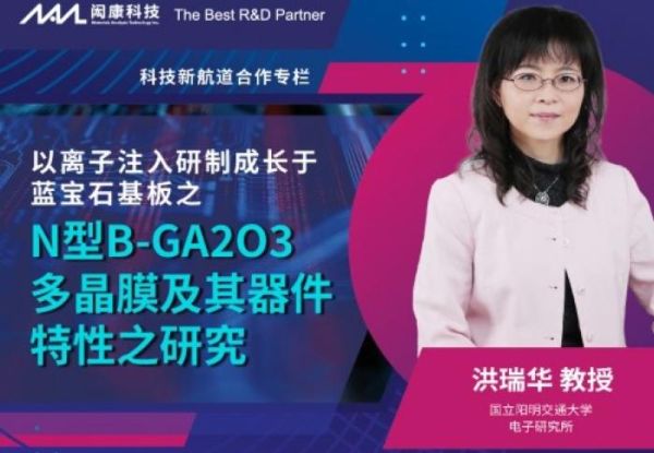
Research on the characteristics of N-type β-Ga2O3 polycrystalline films grown on sapphire substrates by ion implantation and their device properties.
In recent years, the rapid development of electric vehicles and renewable energy has led to an increasing demand and performance requirements for power devices. Silicon (Si) has a bandgap (Eg) of only 1.12 eV, which cannot withstand high voltages. Currently, high-voltage and high-power power devices are gradually adopting third-generation wide bandgap semiconductors, such as silicon carbide (SiC) and gallium nitride (GaN). Devices made from these materials can significantly enhance the voltage and power of power devices, thereby improving applications in electric vehicles and renewable energy.
Analysis of material composition in the assessment of chemical analysis.
For the testing of the provided samples, MA-tek can offer services that typically include testing and analysis of the customer-specified instrument systems, as well as the investigation and analysis of unknown components in the samples or foreign objects.
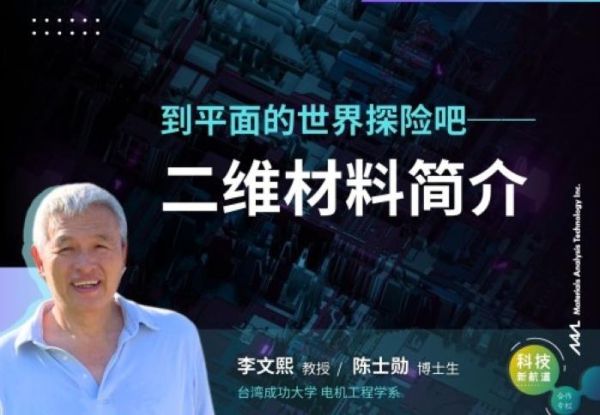
Let's explore the world of planes---Introduction to two-dimensional materials
Two-dimensional material systems have many excellent properties that have been reported. The 2D semiconductor hardware system that integrates sensing, storage, and processing will disrupt the architecture of electronic applications in the future. At this stage, there is still much research work to be done to develop integrated circuit mass production and even commercial applications.
Integrated Circuit Electrostatic Protection and Latch-up Testing Plan and Failure Verification Process
In the product development stage, ESD and LU testing and analysis are indispensable parts. Following the verification process outlined in this article can quickly resolve certification issues. If there are any other special circumstances, please feel free to contact MA-tek's professional team for more in-depth analysis.